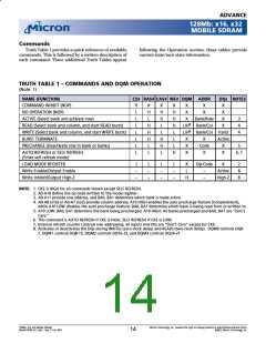
ADVANCE
128Mb: x16, x32
MOBILE SDRAM
Burst Type
Accesses within a given burst may be programmed to
be either sequential or interleaved; this is referred to as
the burst type and is selected via bit M3.
The ordering of accesses within a burst is determined
by the burst length, the burst type and the starting col-
umn address, as shown in Table 1.
Table 1
Burst Definition
Burst
Length
Starting Column Order of Accesses Within a Burst
Address
Type = Sequential Type = Interleaved
A0
0
1
0-1
1-0
0-1
1-0
2
4
A1 A0
Figure 1
Mode Register Definition
0
0
1
1
0
1
0
1
0-1-2-3
1-2-3-0
2-3-0-1
3-0-1-2
0-1-2-3
1-0-3-2
2-3-0-1
3-2-1-0
Address Bus
BA1 BA0 A11 A10 A9 A8
A7 A6 A5 A4
A3 A2 A1 A0
A2 A1 A0
M13 M12 M11 M10 M9 M8 M7 M6 M5 M4 M3 M2 M1 M0
13 12
0
0
0
0
1
1
1
1
0
0
1
1
0
0
1
1
0
1
0
1
0
1
0
1
0-1-2-3-4-5-6-7
1-2-3-4-5-6-7-0
2-3-4-5-6-7-0-1
3-4-5-6-7-0-1-2
4-5-6-7-0-1-2-3
5-6-7-0-1-2-3-4
6-7-0-1-2-3-4-5
7-0-1-2-3-4-5-6
Cn, Cn + 1, Cn + 2
Cn + 3, Cn + 4...
…Cn - 1,
0-1-2-3-4-5-6-7
1-0-3-2-5-4-7-6
2-3-0-1-6-7-4-5
3-2-1-0-7-6-5-4
4-5-6-7-0-1-2-3
5-4-7-6-1-0-3-2
6-7-4-5-2-3-0-1
7-6-5-4-3-2-1-0
9
8
6
5
4
1
11 10
7
3
2
0
Mode Register (Mx)
Reserved* WB Op Mode CAS Latency
BT
Burst Length
Reserved**
8
Burst Length
*Should program
M10 = “0, 0”
to ensure compatibility
with future devices.
M2 M1 M0
M3 = 0
M3 = 1
0
0
0
0
1
1
1
1
0
0
1
1
0
0
1
1
0
1
0
1
0
1
0
1
1
2
1
2
4
4
8
8
** BA1, BA0 = “0, 0”
to prevent Extended
Mode Register.
Full
Page
(y)
n = A0-A11
Reserved
Reserved
Reserved
Full Page
Reserved
Reserved
Reserved
Reserved
Not Supported
(location 0-y)
Cn…
NOTE: 1. For full-page accesses: y = 512 (x16), y = 256
(x32).
Burst Type
M3
0
Sequential
Interleaved
2. For a burst length of two, A1-A8 (x16) or A1-A7
(x32) select the block-of-two burst; A0 selects
the starting column within the block.
3. For a burst length of four, A2-A8 (x16) or A2-A7
(x32) select the block-of-four burst; A0-A1 select
the starting column within the block.
4. For a burst length of eight, A3-A8 (x16) or A3-
A7 (x32) select the block-of-eight burst; A0-A2
select the starting column within the block.
5. For a full-page burst, the full row is selected
and A0-A8 (x16) or A0-A7 (x32) select the
starting column.
6. Whenever a boundary of the block is reached
within a given sequence above, the following
access wraps within the block.
1
CAS Latency
M6 M5 M4
Reserved
1
0
0
0
0
1
1
1
1
0
0
1
1
0
0
1
1
0
1
0
1
0
1
0
1
2
3
Reserved
Reserved
Reserved
Reserved
M8
0
M7
0
M6-M0
Defined
-
Operating Mode
Standard Operation
All other states reserved
-
-
7. For a burst length of one, A0-A8 (x16) or A0-A7
(x32) select the unique column to be accessed,
and mode register bit M3 is ignored.
Write Burst Mode
M9
0
Programmed Burst Length
Single Location Access
1
128Mb: x16, x32 Mobile SDRAM
MobileY95W_3V_F.p65 – Rev. F; Pub. 9/02
Micron Technology, Inc., reserves the right to change products or specifications without notice.
©2002, Micron Technology, Inc.
10

 MICRON [ MICRON TECHNOLOGY ]