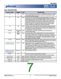
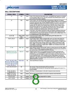
ADVANCE
128Mb: x16, x32
MOBILE SDRAM
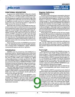
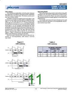
CAS Latency
Operating Mode
The CAS latency is the delay, in clock cycles, between
the registration of a READ command and the availability
of the first piece of output data. The latency can be set to
one, two, or three clocks.
The normal operating mode is selected by setting M7
and M8 to zero; the other combinations of values for M7
and M8 are reserved for future use and/or test modes.
The programmed burst length applies to both READ and
WRITE bursts.
Test modes and reserved states should not be used
because unknown operation or incompatibility with fu-
ture versions may result.
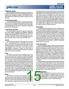
If a READ command is registered at clock edge n, and
the latency is m clocks, the data will be available by clock
edge n + m. The DQs will start driving as a result of the
clock edge one cycle earlier (n + m - 1), and provided that
the relevant access times are met, the data will be valid by
clock edge n + m. For example, assuming that the clock
cycle time is such that all relevant access times are met,
if a READ command is registered at T0 and the latency is
programmed to two clocks, the DQs will start driving
after T1 and the data will be valid by T2, as shown in
Figure 2. Table 2 indicates the operating frequencies at
which each CAS latency setting can be used.
Reserved states should not be used as unknown op-
eration or incompatibility with future versions
may result.
Figure 2
CAS Latency
Table 2
CAS Latency
T0
T1
T2
CLK
ALLOWABLE OPERATING
FREQUENCY (MHz)
COMMAND
READ
NOP
t
CAS
CAS
CAS
t
LZ
OH
SPEED
- 8
LATENCY = 1 LATENCY = 2 LATENCY = 3
D
OUT
DQ
t
AC
≤ 50
≤ 40
≤ 100
≤ 83
≤ 125
≤ 100
- 10
CAS Latency = 1
T0
T1
T2
T3
CLK
COMMAND
READ
NOP
t
NOP
t
LZ
OH
D
OUT
DQ
t
AC
CAS Latency = 2
T0
T1
T2
T3
T4
CLK
COMMAND
READ
NOP
NOP
NOP
t
t
LZ
OH
D
OUT
DQ
t
AC
CAS Latency = 3
DON’T CARE
UNDEFINED
128Mb: x16, x32 Mobile SDRAM
MobileY95W_3V_F.p65 – Rev. F; Pub. 9/02
Micron Technology, Inc., reserves the right to change products or specifications without notice.
©2002, Micron Technology, Inc.
11

 MICRON [ MICRON TECHNOLOGY ]