ADVANCE
128Mb: x16, x32
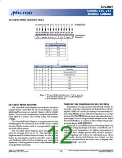
MOBILE SDRAM
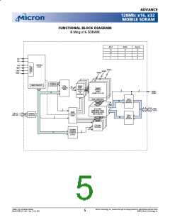
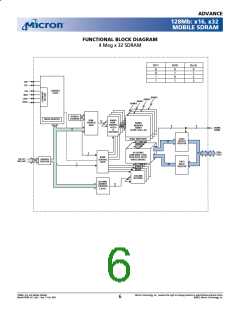
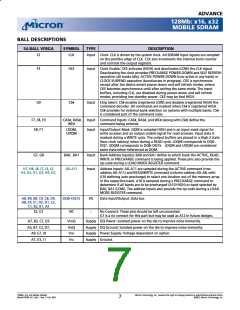
BALL DESCRIPTIONS
90-BALL FBGA
SYMBOL
TYPE
DESCRIPTION
J1
CLK
Input Clock: CLK is driven by the system clock. All SDRAM input signals are sampled
on the positive edge of CLK. CLK also increments the internal burst counter
and controls the output registers.
J2
CKE
Input Clock Enable: CKE activates (HIGH) and deactivates (LOW) the CLK signal.
Deactivating the clock provides PRECHARGE POWER-DOWN and SELF REFRESH
operation (all banks idle), ACTIVE POWER-DOWN (row active in any bank) or
CLOCK SUSPEND operation (burst/access in progress). CKE is synchronous
except after the device enters power-down and self refresh modes, where
CKE becomes asynchronous until after exiting the same mode. The input
buffers, including CLK, are disabled during power-down and self refresh
modes, providing low standby power. CKE may be tied HIGH.
J8
CS#
Input Chip Select: CS# enables (registered LOW) and disables (registered HIGH) the
command decoder. All commands are masked when CS# is registered HIGH.
CS# provides for external bank selection on systems with multiple banks. CS#
is considered part of the command code.
J9, K7, K8
RAS#, CAS#
WE#
Input Command Inputs: RAS#, CAS#, and WE# (along with CS#) define the
command being entered.
K9, K1, F8, F2
DQM0–3
Input Input/Output Mask: DQM is sampled HIGH and is an input mask signal for
write accesses and an output enable signal for read accesses. Input data is
masked during a WRITE cycle. The output buffers are placed in a High-Z state
(two-clock latency) when during a READ cycle. DQM0 corresponds to DQ0–
DQ7, DQM1 corresponds to DQ8–DQ15, DQM2 corresponds to DQ16–DQ23
and DQM3 corresponds to DQ24–DQ31. DQM0-3 are considered same state
when referenced as DQM.
J7, H8
BA0, BA1
A0–A11
Input Bank Address Input(s): BA0 and BA1 define to which bank the ACTIVE, READ,
WRITE or PRECHARGE command is being applied. These pins also provide the
op-code during a LOAD MODE REGISTER command
G8, G9, F7, F3, G1, G2,
G3, H1, H2, J3, G7, H9
Input Address Inputs: A0–A11 are sampled during the ACTIVE command (row-
address A0–A11) and READ/WRITE command (column-address A0–A7; with
A10 defining auto precharge) to select one location out of the memory array
in the respective bank. A10 is sampled during a PRECHARGE command to
determine if all banks are to be precharged (A10 HIGH) or bank selected by
BA0, BA1 (LOW). The address inputs also provide the op-code during a LOAD
MODE REGISTER command.
R8, N7, R9, N8, P9, M8,
M7, L8, L2, M3, M2, P1, N2,
R1, N3, R2, E8, D7, D8, B9,
C8, A9, C7, A8, A2, C3, A1,
C2, B1, D2, D3, E2
DQ0–DQ31
I/O
Data Input/Output: Data bus
E3, E7, H3, H7, K2, K3
NC
–
No Connect: These pins should be left unconnected.
H7 and H9 are not connects for this part but may be used as A12 and A11 in
future designs.
B2, B7, C9, D9, E1,
L1, M9, N9, P2, P7
VDDQ
VSSQ
Supply DQ Power: Isolated power on the die to improve noise immunity.
B8, B3, C1, D1, E9,
L9, M1, N1, P3, P8
Supply DQ Ground: Isolated power on the die to improve noise immunity.
A7, F9, L7, R7
A3, F1, L3, R3
VDD
VSS
Supply Power Supply: Voltage dependant on option.
Supply Ground.
128Mb: x16, x32 Mobile SDRAM
Micron Technology, Inc., reserves the right to change products or specifications without notice.
MobileY95W_3V_F.p65 – Rev. F; Pub. 9/02
©2002, Micron Technology, Inc.
8

 MICRON [ MICRON TECHNOLOGY ]