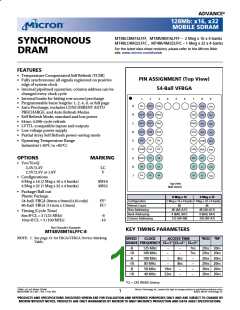
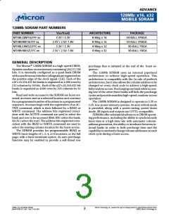
ADVANCE
128Mb: x16, x32
MOBILE SDRAM
TABLE OF CONTENTS
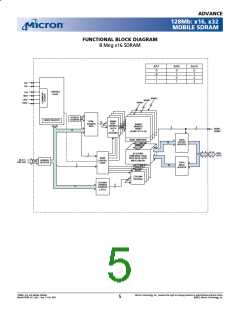
Functional Block Diagram – 8 Meg x 16 ................
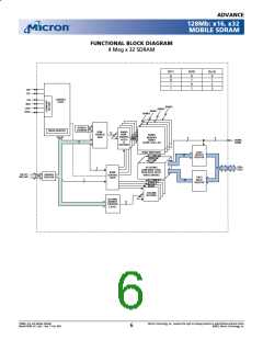
Functional Block Diagram – 4 Meg x 32 ................
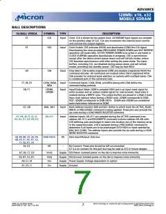
54-Ball Pin Descriptions .........................................
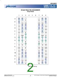
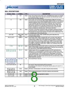
90-Ball Pin Descriptions .........................................
5
6
7
8
Truth Table 2 (CKE) ................................................ 30
Truth Table 3 (Current State, Same Bank) ..................... 31
Truth Table 4 (Current State, Different Bank) ................. 33
Absolute Maximum Ratings ................................... 35
DC Electrical Characteristics
Functional Description .........................................
Initialization ......................................................
Register Definition ............................................
mode register ................................................
Burst Length............................................
9
9
9
9
9
and Operating Conditions ................................... 35
AC Electrical Characteristics and Recommended
Operating Conditions (Timing Table) ............. 36
AC Functional Characteristics ................................ 37
IDD Specifications and Conditions ......................... 37
Capacitance ............................................................ 38
Burst Type ............................................... 10
CAS Latency ............................................ 11
Operating Mode ...................................... 11
Extended Mode Register ......................... 12
Timing Waveforms
Initialize and Load mode register...................... 40
Power-Down Mode ............................................ 41
Clock Suspend Mode ......................................... 42
Auto Refresh Mode ............................................ 43
Self Refresh Mode .............................................. 44
Reads
Read – Without Auto Precharge ................... 45
Read – With Auto Precharge ........................ 46
Single Read – Without Auto Precharge ........ 47
Single Read – With Auto Precharge ............. 48
Alternating Bank Read Accesses ................... 49
Read – Full-Page Burst .................................. 50
Read – DQM Operation ................................ 51
Writes
Temperature Compensated Self Refresh . 12
Partial Array Self Refresh......................... 13
Commands ............................................................. 14
Truth Table 1 (Commands and DQM Operation) ............ 14
Command Inhibit ............................................. 15
No Operation (NOP).......................................... 15
Load mode register ............................................ 15
Active ................................................................ 15
Read ................................................................ 15
Write ................................................................ 15
Precharge ........................................................... 15
Auto Precharge .................................................. 15
Burst Terminate ................................................. 15
Auto Refresh ...................................................... 16
Self Refresh ........................................................ 16
Operation................................................................ 17
Bank/Row Activation ........................................ 17
Reads ................................................................ 18
Writes ................................................................ 24
Precharge ........................................................... 26
Concurrent Auto Precharge .............................. 28
Power-Down ...................................................... 26
Clock Suspend ................................................... 27
Burst Read/Single Write .................................... 27
Write – Without Auto Precharge ................. 52
Write – With Auto Precharge ....................... 53
Single Write – Without Auto Precharge....... 54
Single Write – With Auto Precharge ............ 55
Alternating Bank Write Accesses ................. 56
Write – Full-Page Burst ................................. 57
Write – DQM Operation .............................. 58
54-Ball VFBGA Drawing ............................... 59
90-Ball FBGA Drawing ................................. 60
FBGA/VFBGA Device Marking ..................... 61
128Mb: x16, x32 Mobile SDRAM
MobileY95W_3V_F.p65 – Rev. F; Pub. 9/02
Micron Technology, Inc., reserves the right to change products or specifications without notice.
©2002, Micron Technology, Inc.
4

 MICRON [ MICRON TECHNOLOGY ]