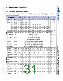
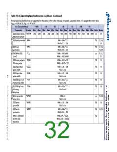
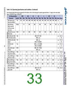
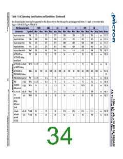
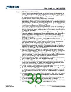
Table 11: AC Operating Specifications and Conditions (Continued)
Not all speed grades listed may be supported for this device; refer to the title page for speeds supported; Notes: 1–5 apply to the entire table;
VDDQ = +1.8V ±0.1V, VDD = +1.8V ±0.1V
AC Characteristics
-187E
-25E
-25
-3E
-3
-37E
-5E
Parameter
Symbol Min Max Min Max Min Max Min Max Min Max Min Max Min Max Units Notes
Input setup time
Input hold time
Input setup time
Input hold time
Input pulse width
tISb
tIHb
tISa
tIHa
tIPW
tRC
125
200
325
325
0.6
175
250
375
375
0.6
175
250
375
375
0.6
200
275
400
400
0.6
200
275
400
400
0.6
250
375
500
500
0.6
350
475
600
600
0.6
ps
ps
ps
ps
31, 33
31, 33
31, 33
31, 33
–
–
–
–
–
–
–
–
–
–
–
–
–
–
–
–
–
–
–
–
–
–
–
–
–
–
–
–
–
–
–
–
–
–
–
–
–
–
–
–
–
–
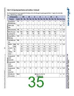
tCK 18, 32
ACTIVATE-to-
ACTIVATE delay,
same bank
54
55
55
54
55
55
55
ns
18, 34
ACTIVATE-to-READ
or WRITE delay
tRCD
tRAS
13.125
40
12.5
40
15
40
12
40
15
40
15
40
15
40
ns
ns
18
–
–
–
–
–
–
–
ACTIVATE-to-
PRECHARGE delay
70K
70K
70K
70K
70K
70K
70K
18, 34,
35
PRECHARGE period
tRP
tRPA
tRPA
13.125
13.125
15
12.5
12.5
15
15
15
12
12
15
15
15
18
15
15
15
15
20
ns
ns
ns
18, 36
18, 36
18, 36
–
–
–
–
–
–
–
–
–
–
–
–
–
–
–
–
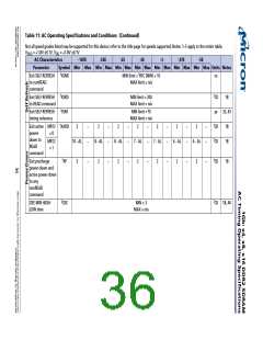
PRE-
<1Gb
CHARGE
ALL period
17.5
18.75
≥1Gb
ACTIVATE x4, x8
tRRD
tRRD
7.5
10
7.5
10
7.5
10
7.5
10
7.5
10
7.5
10
7.5
10
ns
ns
18, 37
18, 37
–
–
–
–
–
–
–
–
–
–
–
–
–
–
-to-
x16
ACTIVATE
delay
different
bank
4-bank
activate
period
(≥1Gb)
x4, x8
x16
tFAW
tFAW
35
45
35
45
35
45
37.5
50
37.5
50
37.5
50
37.5
50
ns
ns
18, 38
18, 38
–
–
–
–
–
–
–
–
–
–
–
–
–
–

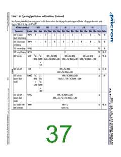
 MICRON [ MICRON TECHNOLOGY ]