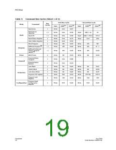
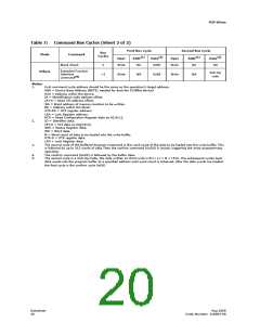
P33-65nm
8.0
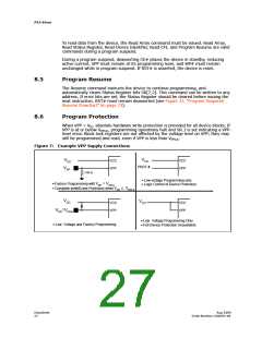
Program Operation
The device supports three programming methods: Word Programming (40h or 10h),
Buffered Programming (E8h, D0h), and Buffered Enhanced Factory Programming (80h,
D0h). The following sections describe device programming in detail.
Successful programming requires the addressed block to be unlocked. If the block is
locked down, WP# must be deasserted and the block must be unlocked before
attempting to program the block. Attempting to program a locked block causes a
program error (SR.4 and SR.1 set) and termination of the operation. See Section 10.0,
“Security” on page 30 for details on locking and unlocking blocks.
8.1
Word Programming
Word programming operations are initiated by writing the Word Program Setup
command to the device. This is followed by a second write to the device with the
address and data to be programmed. The device outputs Status Register data when
read. See Figure 31, “Word Program Flowchart” on page 72. VPP must be above VPPLK
,
and within the specified VPPL min/max values.
During programming, the WSM executes a sequence of internally-timed events that
program the desired data bits at the addressed location, and verifies that the bits are
sufficiently programmed. Programming the flash memory array changes “ones” to
“zeros”. Memory array bits that are zeros can be changed to ones only by erasing the
block.
The Status Register can be examined for programming progress and errors by reading
at any address. The device remains in the Read Status Register state until another
command is written to the device.
Status Register bit SR.7 indicates the programming status while the sequence
executes. Commands that can be issued to the device during programming are
Program Suspend, Read Status Register, Read Device Identifier, Read CFI, and Read
Array (this returns unknown data).
When programming has finished, Status Register bit SR.4 (when set) indicates a
programming failure. If SR.3 is set, the WSM could not perform the word programming
operation because VPP was outside of its acceptable limits. If SR.1 is set, the word
programming operation attempted to program a locked block, causing the operation to
abort.
Before issuing a new command, the Status Register contents should be examined and
then cleared using the Clear Status Register command. Any valid command can follow,
when word programming has completed.
8.2
Buffered Programming
The device features a 512-word buffer to enable optimum programming performance.
For Buffered Programming, data is first written to an on-chip write buffer. Then the
buffer data is programmed into the flash memory array in buffer-size increments. This
can improve system programming performance significantly over non-buffered
programming. (see Figure 33, “Buffer Program Flowchart” on page 74).
When the Buffered Programming Setup command is issued, Status Register information
is updated and reflects the availability of the buffer. SR.7 indicates buffer availability: if
set, the buffer is available; if cleared, the buffer is not available.
Note:
The device default state is to output SR data after the Buffer Programming Setup
Command. CE# and OE# low drive device to update Status Register. It is not allowed
Datasheet
23
Aug 2009
OrderNumber:320003-08

 MICRON [ MICRON TECHNOLOGY ]