P33-65nm
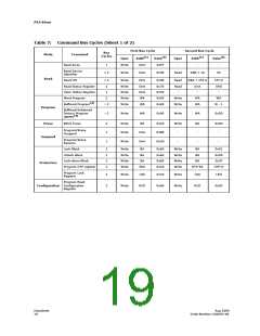
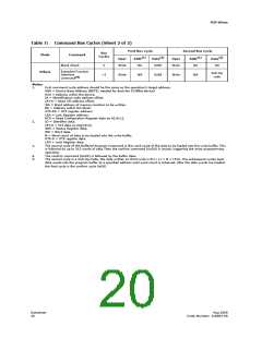
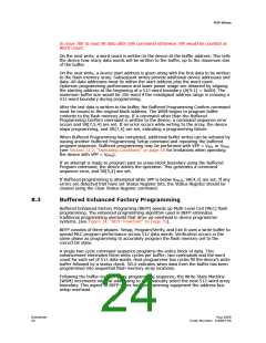
Table 7:
Command Bus Cycles (Sheet 2 of 2)
First Bus Cycle
Second Bus Cycle
Bus
Mode
Command
Cycles
(1)
(2)
(1)
(2)
Oper
Addr
Data
Oper
Addr
Data
Blank Check
2
Write
BA
0xBC
Write
BA
D0
Extended Function
Interface
Others
Sub-Op
code
>2
Write
WA
0xEB
Write
WA
(5)
command
Notes:
1.
First command cycle address should be the same as the operation’s target address.
DBA = Device Base Address (NOTE: needed for dual-die 512Mbit device)
DnA = Address within the device.
IA = Identification code address offset.
CFI-A = Read CFI address offset.
WA = Word address of memory location to be written.
BA = Address within the block.
OTP-RA = OTP register address.
LRA = Lock Register address.
RCD = Read Configuration Register data on A[16:1].
ID = Identifier data.
2.
3.
CFI-D = CFI data on DQ[15:0].
SRD = Status Register data.
WD = Word data.
N = Word count of data to be loaded into the write buffer.
OTP-D = OTP register data.
LRD = Lock Register data.
The second cycle of the Buffered Program Command is the word count of the data to be loaded into the write buffer. This
is followed by up to 512 words of data.Then the confirm command (0xD0) is issued, triggering the array programming
operation.
4.
5.
The confirm command (0xD0) is followed by the buffer data.
The second cycle is a Sub-Op-Code, the data written on third cycle is N-1; 1=< N <=512. The subsequent cycles load
data words into the program buffer at a specified address until word count is achieved, after the data words are loaded,
the final cycle is the confirm cycle 0xD0)
Datasheet
20
Aug 2009
Order Number: 320003-08

 MICRON [ MICRON TECHNOLOGY ]