P33-65nm
5.0
Bus Operations
CE# low and RST# high enable device read operations. The device internally decodes
upper address inputs to determine the accessed block. ADV# low opens the internal
address latches. OE# low activates the outputs and gates selected data onto the I/O
bus.
In asynchronous mode, the address is latched when ADV# goes high or continuously
flows through if ADV# is held low. In synchronous mode, the address is latched by the
first of either the rising ADV# edge or the next valid CLK edge with ADV# low (WE#
and RST# must be VIH; CE# must be VIL).
Bus cycles to/from the P33-65nm device conform to standard microprocessor bus
operations. Table 5, “Bus Operations Summary”summarizes the bus operations and the
logic levels that must be applied to the device control signal inputs.
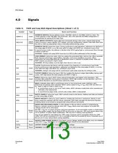
Table 5:
Bus Operations Summary
Bus Operation
RST#
CLK
ADV#
CE#
OE#
WE#
WAIT
DQ[15:0] Notes
Asynchronous
Synchronous
V
V
V
V
V
X
L
L
L
L
L
L
H
H
L
Output
Output
IH
Deasserted
Driven
Read
Write
Running
IH
IH
IH
IH
X
X
X
X
L
L
H
H
X
X
High-Z
High-Z
High-Z
High-Z
Input
High-Z
High-Z
High-Z
1
2
Output Disable
Standby
Reset
X
X
X
L
H
X
X
H
X
2
V
2,3
IL
Notes:
1.
Refer to the Table 7, “Command Bus Cycles” on page 19 for valid DQ[15:0] during a write
operation.
2.
3.
X = Don’t Care (H or L).
RST# must be at V ± 0.2 V to meet the maximum specified power-down current.
SS
5.1
5.2
Read
To perform a read operation, RST# and WE# must be deasserted while CE# and OE#
are asserted. CE# is the device-select control. When asserted, it enables the flash
memory device. OE# is the data-output control. When asserted, the addressed flash
memory data is driven onto the I/O bus.
Write
To perform a write operation, both CE# and WE# are asserted while RST# and OE# are
deasserted. During a write operation, address and data are latched on the rising edge
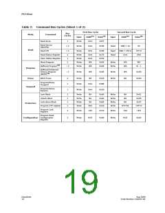
of WE# or CE#, whichever occurs first. Table 7, “Command Bus Cycles” on page 19
shows the bus cycle sequence for each of the supported device commands, while
Table 6, “Command Codes and Definitions” on page 17 describes each command. See
Section 15.0, “AC Characteristics” on page 48 for signal-timing details.
Note:
Write operations with invalid VCC and/or VPP voltages can produce spurious results and
should not be attempted.
5.3
Output Disable
When OE# is deasserted, device outputs DQ[15:0] are disabled and placed in a high-
impedance (High-Z) state, WAIT is also placed in High-Z.
Datasheet
15
Aug 2009
OrderNumber:320003-08

 MICRON [ MICRON TECHNOLOGY ]