P33-65nm
4.0
Signals
Table 4:
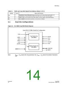
TSOP and Easy BGA Signal Descriptions (Sheet 1 of 2)
Symbol
Type
Name and Function
ADDRESS INPUTS: Device address inputs. 256-Mbit: A[24:1]; 512-Mbit: A[25:1]. Note: The
A[MAX:1]
DQ[15:0]
Input
virtual selection of the 256-Mbit “Top parameter” die in the dual-die 512-Mbit configuration is
accomplished by setting A[25] high (V ).
IH
DATA INPUT/OUTPUTS: Inputs data and commands during write cycles; outputs data during
reads of memory, status register, OTP register, and read configuration register. Data balls float when
the CE# or OE# are deasserted. Data is internally latched during writes.
Input/
Output
ADDRESS VALID: Active low input. During synchronous read operations, addresses are latched on
the rising edge of ADV#, or on the next valid CLK edge with ADV# low, whichever occurs first.
ADV#
Input
In asynchronous mode, the address is latched when ADV# going high or continuously flows through
if ADV# is held low.
WARNING: Designs not using ADV# must tie it to VSS to allow addresses to flow through.
CHIP ENABLE: Active low input. CE# low selects the associated flash memory die. When asserted,
flash internal control logic, input buffers, decoders, and sense amplifiers are active. When
deasserted, the associated flash die is deselected, power is reduced to standby levels, data and
WAIT outputs are placed in high-Z state.
CE#
CLK
Input
Input
WARNING: All chip enables must be high when device is not in use.
CLOCK: Synchronizes the device with the system’s bus frequency in synchronous-read mode.
During synchronous read operations, addresses are latched on the rising edge of ADV#, or on the
next valid CLK edge with ADV# low, whichever occurs first.
WARNING: Designs not using CLK for synchronous read mode must tie it to VCCQ or VSS.
OUTPUT ENABLE: Active low input. OE# low enables the device’s output data buffers during read
OE#
Input
Input
cycles. OE# high places the data outputs and WAIT in High-Z.
RESET: Active low input. RST# resets internal automation and inhibits write operations. This
provides data protection during power transitions. RST# high enables normal operation. Exit from
reset places the device in asynchronous read array mode.
RST#
WAIT: Indicates data valid in synchronous array or non-array burst reads. RCR[10], (WT)
determines its polarity when asserted. WAIT’s active output is V or V
when CE# and OE# are
OL
OH
V . WAIT is high-Z if CE# or OE# is V
.
IL
IH
WAIT
Output
•
In synchronous array or non-array read modes, WAIT indicates invalid data when asserted and
valid data when deasserted.
•
In asynchronous page mode, and all write modes, WAIT is deasserted.
WRITE ENABLE: Active low input. WE# controls writes to the device. Address and data are latched
on the rising edge of WE#.
WE#
WP#
Input
Input
WRITE PROTECT: Active low input. WP# low enables the lock-down mechanism. Blocks in lock-
down cannot be unlocked with the Unlock command. WP# high overrides the lock-down function
enabling blocks to be erased or programmed using software commands.
ERASE AND PROGRAM POWER: A valid voltage on this pin allows erasing or programming.
Memory contents cannot be altered when VPP ≤ V
voltages should not be attempted.
. Block erase and program at invalid VPP
PPLK
Set VPP = V
for in-system program and erase operations. To accommodate resistor or diode drops
PPL
Power/
Input
VPP
from the system supply, the V level of VPP can be as low as V
min. VPP must remain above V
IH
PPL PPL
min to perform in-system flash modification. VPP may be 0 V during read operations.
V
can be applied to main blocks for 1000 cycles maximum and to parameter blocks for 2500
PPH
cycles. VPP can be connected to 9 V for a cumulative total not to exceed 80 hours. Extended use of
this pin at 9 V may reduce block cycling capability.
DEVICE CORE POWER SUPPLY: Core (logic) source voltage. Writes to the flash array are inhibited
VCC
Power
when VCC ≤ V
. Operations at invalid VCC voltages should not be attempted.
LKO
VCCQ
VSS
Power
Power
OUTPUT POWER SUPPLY: Output-driver source voltage.
GROUND: Connect to system ground. Do not float any VSS connection.
Datasheet
13
Aug 2009
OrderNumber:320003-08

 MICRON [ MICRON TECHNOLOGY ]