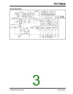
TC7109/A
2.0
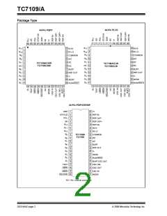
PIN DESCRIPTIONS
The descriptions of the pins are listed in Table 2-1.
TABLE 2-1:
PIN FUNCTION TABLE
Pin Number
(40-Pin PDIP)
Symbol
Description
1
2
GND
Digital ground, 0V, ground return for all digital logic.
STATUS
Output HIGH during integrate and de-integrate until data is latched. Output LOW when
analog section is in auto-zero or zero integrator configuration.
3
4
POL
OR
Polarity – High for positive input.
Over Range – High if over ranged (Three-State Data bit).
Bit 12 (Most Significant bit) (Three-State Data bit).
Bit 11 (Three-State Data bit).
5
B
B
B
12
11
10
6
7
Bit 10 (Three-State Data bit).
8
B
Bit 9 (Three-State Data bit).
9
8
7
6
5
4
3
2
1
9
B
Bit 8 (Three-State Data bit).
10
11
12
13
14
15
16
17
B
B
B
B
B
B
B
Bit 7 (Three-State Data bit).
Bit 6 (Three-State Data bit).
Bit 5 (Three-State Data bit).
Bit 4 (Three-State Data bit).
Bit 3 (Three-State Data bit).
Bit 2 (Three-State Data bit).
Bit 1 (Least Significant bit) (Three-State Data bit).
TEST
Input High – Normal operation. Input LOW – Forces all bit outputs HIGH.
Note: This input is used for test purposes only.
18
19
20
21
LBEN
Low Byte Enable – with MODE (Pin 21) LOW, and CE/LOAD (Pin 20) LOW, taking this pin
LOW activates low order byte outputs, B –B . With MODE (Pin 21) HIGH, this pin serves as
1
8
low byte flag output used in Handshake mode. (See Figure 3-7, Figure , and Figure 3-9.)
HBEN
CE/LOAD
MODE
High Byte Enable – with MODE (Pin 21) LOW, and CE/LOAD (Pin 20) LOW, taking this pin
LOW activates high order byte outputs, B –B , POL, OR. With MODE (Pin 21) HIGH, this
9
12
pin serves as high byte flag output used in Handshake mode. See Figures 3-7, 3-8, and 3-9.
Chip Enable/Load – with MODE (Pin 21) LOW, CE/LOAD serves as a master output enable.
When HIGH, B –B , POL, OR outputs are disabled. When MODE (Pin 21) is HIGH, a load
1
12
strobe is used in handshake mode. (See Figure 3-7, Figure , and Figure 3-9.)
Input LOW – Direct Output mode where CE/LOAD (Pin 20), HBEN (Pin 19), and LBEN (Pin
18) act as inputs directly controlling byte outputs. Input Pulsed HIGH - Causes immediate
entry into Handshake mode and output of data as in Figure 3-9.
Input HIGH – enables CE/LOAD (Pin 20), HBEN (Pin 19), and LBEN (Pin 18) as outputs,
Handshake mode will be entered and data output as in Figure 3-7 and Figure 3-9
at conversions completion.
22
23
24
OSC IN
OSC OUT
OSC SEL
Oscillator Input.
Oscillator Output.
Oscillator Select – Input HIGH configures OSC IN, OSC OUT, BUFF OSC OUT as RC
oscillator – clock will be same phase and duty cycle as BUFF OSC OUT. Input LOW
configures OSC IN, OSC OUT for crystal oscillator - clock frequency will be 1/58 of frequency
at BUFF OSC OUT.
25
26
BUFF OSC OUT Buffered Oscillator Output.
RUN/HOLD
Input HIGH – Conversions continuously performed every 8192 clock pulses.
Input LOW – Conversion in progress completed; converter will stop in auto-zero seven
counts before integrate.
27
SEND
Input - Used in Handshake mode to indicate ability of an external device to accept data.
Connect to V+ if not used.
28
29
V-
Analog Negative Supply – Nominally -5V with respect to GND (Pin 1).
Reference Voltage Output – Nominally 2.8V down from V+ (Pin 40).
REF OUT
DS21456C-page 6
© 2006 Microchip Technology Inc.

 MICROCHIP [ MICROCHIP ]