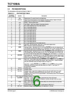
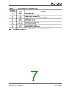
TC7109/A
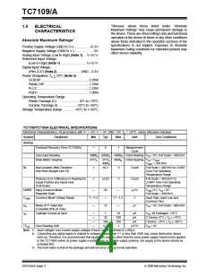
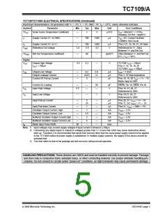
TC7109/TC7109A ELECTRICAL SPECIFICATIONS (Continued)
Electrical Characteristics: All parameters with V+ = +5V, V- = -5V, GND = 0V, T = +25°C, unless otherwise indicated.
A
Symbol
Parameter
Min
Typ
Max
Unit
Test Conditions
TC
Scale Factor Temperature Coefficient
—
1
5
μV/°C
V
= 408.9mV = >7770
8
FS
IN
Reading, Ext Ref = 0ppm/°C
+
Supply Current (V+ to GND)
—
700
1500
μA
V
IN
= 0V, Crystal Oscillator
I
3.58MHz Test Circuit
I
Supply Current (V+ to V-)
Reference Out Voltage
—
700
-2.8
1500
-3.2
μA
Pins 2-21, 25, 26, 27, 29 Open
S
V
-2.4
V
Referenced to V+, 25kΩ
REF
Between V+ and Ref Out
TC
Ref Out Temperature Coefficient
—
80
—
—
ppm/°C
V
25kΩ Between V+ and Ref Out
REF
0°C ≤ T ≤ +70°C
A
Digital
V
Output High Voltage
3.5
4.3
TC7109: I
= 100μA
OUT
OH
I
= 700μA
Pins 3 -16, 18, 19, 20
OUT
TC7109A: I = 700μA
OUT
V
Output Low Voltage
—
—
—
0.2
±0.01
5
0.4
±1
—
μA
μA
μF
I
= 1.6mA
OUT
OL
Output Leakage Current
Control I/O Pull-up Current
Pins 3 -16 High-Impedance
Pins 18, 19, 20 V = V+ – 3V
OUT
Mode Input at GND
Control I/O Loading
Input High Voltage
—
—
—
50
—
pF
V
HBEN, Pin 19; LBEN, Pin 18
V
V
2.5
Pins 18 -21, 26, 27
Referenced to GND
IH
Input Low Voltage
—
—
1
V
Pins 18-21, 26, 27
Referenced to GND
IL
Input Pull-up Current
—
—
5
25
—
—
μA
μA
Pins 26, 27; V
Pins 17, 24; V
= V+ – 3V
= V+ – 3V
OUT
OUT
Input Pull-down Current
—
—
—
—
—
60
1
1
—
—
—
—
—
—
μA
mA
mA
mA
mA
nsec
Pins 21, V
= GND = +3V
OUT
Oscillator Output Current, High
Oscillator Output Current, Low
Buffered Oscillator Output Current High
Buffered Oscillator Output Current Low
Mode Input Pulse Width
V
V
V
V
– 2.5V
– 2.5V
– 2.5V
– 2.5V
OUT
OUT
OUT
OUT
1.5
2
5
t
—
W
Note 1: Input voltages may exceed supply voltages if input current is limited to ±100μA.
2: Connecting any digital inputs or outputs to voltages greater than V+ or less than GND may cause destructive device
latch-up. Therefore, it is recommended that inputs from sources other than the same power supply should not be applied
to the TC7109A before its power supply is established. In multiple supply systems, the supply to the device should be
activated first.
3: This limit refers to that of the package and will not occur during normal operation.
HANDLING PRECAUTIONS: These devices are CMOS and must be handled correctly to prevent damage. Package
and store only in conductive foam, antistatic tubes, or other conducting material. Use proper antistatic handling pro-
cedures. Do not connect in circuits under “power-on” conditions, as high transients may cause permanent damage.
© 2006 Microchip Technology Inc.
DS21456C-page 5

 MICROCHIP [ MICROCHIP ]