TC7109/A
*Stresses above those listed under “Absolute
Maximum Ratings” may cause permanent damage to
the device. These are stress ratings only and functional
operation of the device at these or any other conditions
above those indicated in the operation sections of the
specifications is not implied. Exposure to Absolute
Maximum Rating conditions for extended periods may
affect device reliability.
1.0
ELECTRICAL
CHARACTERISTICS
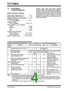
Absolute Maximum Ratings*
Positive Supply Voltage (GND to V+)..................+6.2V
Negative Supply Voltage (GND to V-) .....................-9V
Analog Input Voltage (Low to High) (Note 1).... V+ to V-
Reference Input Voltage:
(Low to High) (Note 1) ............................. V+ to V-
Digital Input Voltage:
(Pins 2-27) (Note 2)...........................GND – 0.3V
Power Dissipation, TA < 70°C (Note 3)
CERDIP ......................................................2.29W
Plastic DIP ..................................................1.23W
PLCC ..........................................................1.23W
PQFP ..........................................................1.00W
Operating Temperature Range
Plastic Package (C) .........................0°C to +70°C
Ceramic Package (I) .....................-25°C to +85°C
Storage Temperature Range..............-65°C to +150°C
TC7109/TC7109A ELECTRICAL SPECIFICATIONS
Electrical Characteristics: All parameters with V+ = +5V, V- = -5V, GND = 0V, T = +25°C, unless otherwise indicated.
A
Symbol
Analog
Parameter
Min
Typ
Max
Unit
Test Conditions
Overload Recovery Time (TC7109A)
—
0
1
Measurement
Cycle
Zero Input Reading
Ratio Metric Reading
-0000 ±0000
+0000
Octal Reading
Octal Reading
V
= 0V; Full Scale = 409.6mV
8
8
8
IN
3777
3777
4000
4000
V
V
= V
REF
= 204.8mV
8
8
8
IN
8
REF
NL
Non-Linearity (Max Deviation
from Best Straight Line Fit)
-1
±0.2
+1
Count
Count
Full Scale = 409.6mV to 2.048V
Over Full Operating
Temperature Range
Rollover Error (Difference in Reading for
Equal Positive and Inputs near
(Full Scale)
-1
±0.02
+1
—
Full Scale = 409.6mV to
2.048V Over Full Operating
Temperature Range
CMRR
Input Common Mode
Rejection Ratio
—
50
—
15
μV/V
V
V
±1V, V = 0V
CM IN
Full Scale = 409.6mV
V
e
Common Mode Voltage Range
V- +1.5
—
V+ -1.5
—
Input High, Input Low and
Common Pins
CMR
Noise (P-P Value Not
μV
V
= 0V, Full Scale = 409.6mV
N
IN
Exceeded 95% of Time)
I
Leakage Current at Input
—
—
—
—
1
10
100
250
1
pA
pA
V
, All Packages: +25°C
IN
IN
20
C Device: 0°C ≤ T ≤ +70°C
I Device: -25°C ≤ T ≤ +85°C
A
100
0.2
pA
A
TC
Zero Reading Drift
μV/°C
V
= 0V
ZS
IN
Note 1: Input voltages may exceed supply voltages if input current is limited to ±100μA.
2: Connecting any digital inputs or outputs to voltages greater than V+ or less than GND may cause destructive device
latch-up. Therefore, it is recommended that inputs from sources other than the same power supply should not be applied
to the TC7109A before its power supply is established. In multiple supply systems, the supply to the device should be
activated first.
3: This limit refers to that of the package and will not occur during normal operation.
DS21456C-page 4
© 2006 Microchip Technology Inc.

 MICROCHIP [ MICROCHIP ]