1 Mbit / 2 Mbit / 4 Mbit Multi-Purpose Flash
SST39SF010A / SST39SF020A / SST39SF040
Data Sheet
T
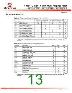
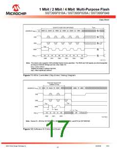
SIX-BYTE CODE FOR CHIP-ERASE
5555 5555 2AAA
SCE
5555
2AAA
5555
ADDRESS A
MS-0
CE#
OE#
WE#
T
WP
AA
55
SW1
80
SW2
AA
SW3
55
SW4
10
DQ
7-0
SW0
SW5
1147 F17.1
Note: This device also supports CE# controlled Sector-Erase operation. The WE# and CE# signals are interchangeable
as long as minimum timings are met. (See Table 10)
SAXX = Sector Address
Toggled bit output is always high first.
AMS = Most significant address
Figure 11:WE# Controlled Chip-Erase Timing Diagram
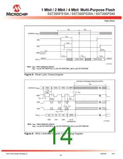
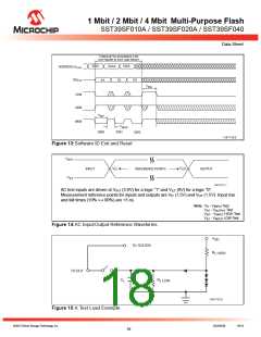
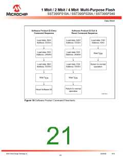
Three-byte Sequence for
Software ID Entry
5555
2AAA
5555
0000
0001
ADDRESS A
14-0
CE#
OE#
WE#
T
IDA
T
WP
T
WPH
T
AA
AA
55
SW1
90
BF
Device ID
DQ
7-0
SW0
SW2
1147 F09.2
Note: Device ID = B5H for SST39SF010A, B6H for SST39SF020A, and B7H for SST39SF040
Figure 12:Software ID Entry and Read
©2013 Silicon Storage Technology, Inc.
DS25022B
04/13
17

 MICROCHIP [ MICROCHIP ]