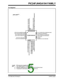
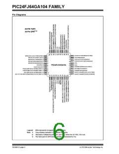
PIC24FJ64GA104 FAMILY
28/44-Pin, 16-Bit General Purpose Flash Microcontrollers
with nanoWatt XLP Technology
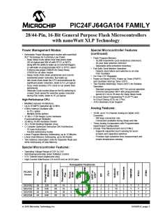
Power Management Modes:
Special Microcontroller Features
(continued):
•
Selectable Power Management modes with nanoWatt
XLP Technology for Extremely Low Power:
•
Flash Program Memory:
-
Deep Sleep mode allows near total power-down
(20 nA typical and 500 nA with RTCC or WDT),
along with the ability to wake-up on external triggers,
or self-wake on programmable WDT or RTCC alarm
Extreme low-power DSBOR for Deep Sleep,
LPBOR for all other modes
Sleep mode shuts down peripherals and core for
substantial power reduction, fast wake-up
Idle mode shuts down the CPU and peripherals for
significant power reduction, down to 4.5 A typical
Doze mode enables CPU clock to run slower than
peripherals
-
-
-
10,000 erase/write cycle endurance (minimum)
20-year data retention minimum
Selectable write protection boundary
•
Fail-Safe Clock Monitor Operation:
-
-
-
-
-
-
Detects clock failure and switches to on-chip
FRC Oscillator
•
•
On-Chip 2.5V Regulator
Power-on Reset (POR), Power-up Timer (PWRT)
and Oscillator Start-up Timer (OST)
Two Flexible Watchdog Timers (WDT) for Reliable
Operation:
•
-
-
Standard programmable WDT for normal operation
Extreme low-power WDT with programmable
period of 2 ms to 26 days for Deep Sleep mode
Alternate Clock modes allow on-the-fly switching to
a lower clock speed for selective power reduction
during Run mode, down to 15 A typical
•
•
In-Circuit Serial Programming™ (ICSP™) and
In-Circuit Debug (ICD) via 2 Pins
JTAG Boundary Scan Support
High-Performance CPU:
•
•
•
Modified Harvard Architecture
Up to 16 MIPS Operation @ 32 MHz
8 MHz Internal Oscillator with:
Analog Features:
-
-
4x PLL option
Multiple divide options
•
10-Bit, up to 13-Channel Analog-to-Digital (A/D)
Converter:
•
17-Bit x 17-Bit Single-Cycle Hardware
Fractional/integer Multiplier
-
-
500 ksps conversion rate
Conversion available during Sleep and Idle
•
•
•
32-Bit by 16-Bit Hardware Divider
16 x 16-Bit Working Register Array
C Compiler Optimized Instruction Set Architecture:
•
•
Three Analog Comparators with Programmable
Input/Output Configuration
Charge Time Measurement Unit (CTMU):
-
-
76 base instructions
Flexible addressing modes
-
-
Supports capacitive touch sensing for touch
screens and capacitive switches
Provides high-resolution time measurement and
simple temperature sensing
•
•
•
Linear Program Memory Addressing, up to 12 Mbytes
Linear Data Memory Addressing, up to 64 Kbytes
Two Address Generation Units for Separate Read and
Write Addressing of Data Memory
Special Microcontroller Features:
•
•
•
•
Operating Voltage Range of 2.0V to 3.6V
Self-Reprogrammable under Software Control
5.5V Tolerant Input (digital pins only)
High-Current Sink/Source (18 mA/18 mA) on All I/O pins
Remappable Peripherals
PIC24FJ
Device
32GA102
64GA102
32GA104
64GA104
28
28
44
44
32K
64K
32K
64K
8K
8K
8K
8K
16
16
26
26
5
5
5
5
5
5
5
5
5
5
5
5
2
2
2
2
2
2
2
2
2
2
2
2
10
10
13
13
3
3
3
3
Y
Y
Y
Y
Y
Y
Y
Y
Y
Y
Y
Y
2010 Microchip Technology Inc.
DS39951C-page 3

 MICROCHIP [ MICROCHIP ]