PIC24FJ64GA104 FAMILY
•
Two UART modules:
Peripheral Features:
-
-
-
-
-
Supports RS-485, RS-232 and LIN/J2602
On-chip hardware encoder/decoder for IrDA®
Auto-wake-up on Start bit
Auto-Baud Detect (ABD)
4-level deep FIFO buffer
•
•
•
Peripheral Pin Select:
-
-
-
Allows independent I/O mapping of many peripherals
Up to 26 available pins (44-pin devices)
Continuous hardware integrity checking and safety
interlocks prevent unintentional configuration changes
•
•
•
•
Five 16-Bit Timers/Counters with Programmable
Prescaler
Five 16-Bit Capture Inputs, each with a Dedicated Time
Base
Five 16-Bit Compare/PWM Outputs, each with a
Dedicated Time Base
Programmable, 32-Bit Cyclic Redundancy Check (CRC)
Generator
8-Bit Parallel Master Port (PMP/PSP):
-
Up to 16-bit multiplexed addressing, with up to
11 dedicated address pins on 44-pin devices
Programmable polarity on control lines
Supports legacy Parallel Slave Port
-
-
Hardware Real-Time Clock/Calendar (RTCC):
-
-
Provides clock, calendar and alarm functions
Functions even in Deep Sleep mode
•
•
Configurable Open-Drain Outputs on Digital I/O Pins
Up to 3 External Interrupt Sources
•
•
Two 3-Wire/4-Wire SPI modules (support 4 Frame
modes) with 8-Level FIFO Buffer
Two I C™ modules support Multi-Master/Slave mode
2
and 7-Bit/10-Bit Addressing
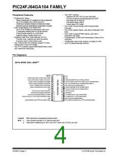
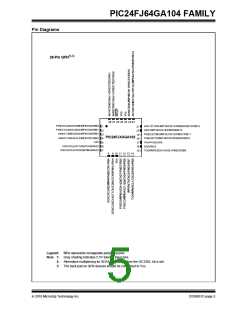
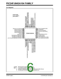
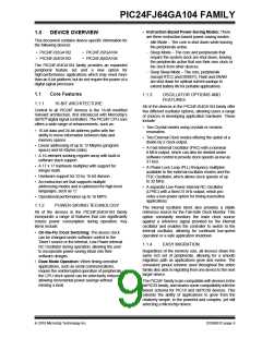
Pin Diagrams
28-Pin SPDIP, SOIC, SSOP(1)
MCLR
1
2
3
4
5
28
27
26
25
24
VDD
VSS
AN0/C3INC/VREF+/CN2/CTED1/RA0
AN1/C3IND/VREF-/CN3/CTED2/RA1
PGED1/AN2/C2INB/RP0/CN4/RB0
PGEC1/AN3/C2INA/RP1/CN5/RB1
AN4/C1INB/RP2/SDA2/CN6/RB2
AN5/C1INA/RP3/SCL2/CN7/RB3
VSS
AN9/C3INA/RP15/CN11/PMCS1/RB15
AN10/C3INB/CVREF/RTCC/RP14/CN12/PMWR/RB14
AN11/C1INC/RP13/CN13/PMRD/REFO/RB13
AN12/RP12/CN14/PMD0/RB12
PGEC2/TMS/RP11/CN15/PMD1/RB11
PGED2/TDI/RP10/CN16/PMD2/RB10
VCAP/VDDCORE
6
7
8
23
22
21
OSCI/CLKI/C1IND/CN30/RA2
OSCO/CLKO/PMA0/CN29/RA3
SOSCI/C2IND/RP4/PMBE/CN1/RB4
SOSCO/SCLKI/T1CK/C2INC/CN0/PMA1/RA4
VDD
9
20
19
18
17
16
15
DISVREG
10
11
12
13
14
TDO/RP9/SDA1/CN21/PMD3/RB9
TCK/RP8/SCL1/CN22/PMD4/RB8
RP7/INT0/CN23/PMD5/RB7
PGC3/EMUC3/RP6/ASCL1(2)/CN24/PMD6/RB6
PGED3/RP5/ASDA1(2)/CN27/PMD7/RB5
Legend:
Note 1: Gray shading indicates 5.5V tolerant input pins.
2: Alternative multiplexing for SDA1 and SCL1 when the I2C1SEL bit is set.
RPn represents remappable peripheral pins.
DS39951C-page 4
2010 Microchip Technology Inc.

 MICROCHIP [ MICROCHIP ]