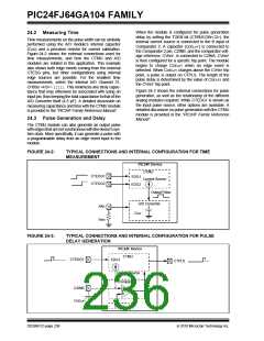
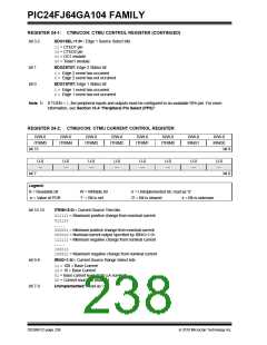
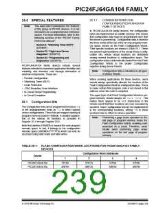
PIC24FJ64GA104 FAMILY
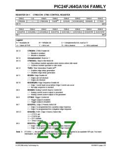
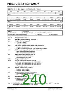
REGISTER 25-1: CW1: FLASH CONFIGURATION WORD 1
U-1
—
U-1
—
U-1
—
U-1
—
U-1
—
U-1
—
U-1
—
U-1
—
bit 23
bit 16
r-x
r
R/PO-1
JTAGEN(1)
R/PO-1
GCP
R/PO-1
GWRP
R/PO-1
DEBUG
U-1
—
R/PO-1
ICS1
R/PO-1
ICS0
bit 15
bit 8
R/PO-1
R/PO-1
WINDIS
U-1
—
R/PO-1
FWPSA
R/PO-1
R/PO-1
R/PO-1
R/PO-1
FWDTEN
WDTPS3
WDTPS2
WDTPS1
WDTPS0
bit 7
bit 0
Legend:
R = Readable bit
-n = Value when device is unprogrammed
r = Reserved bit
PO = Program Once bit
U = Unimplemented bit, read as ‘0’
‘1’ = Bit is set ‘0’ = Bit is cleared
bit 23-16
bit 15
Unimplemented: Read as ‘1’
Reserved: The value is unknown; program as ‘0’
JTAGEN: JTAG Port Enable bit(1)
bit 14
1= JTAG port is enabled
0= JTAG port is disabled
bit 13
bit 12
bit 11
GCP: General Segment Program Memory Code Protection bit
1= Code protection is disabled
0= Code protection is enabled for the entire program memory space
GWRP: General Segment Code Flash Write Protection bit
1= Writes to program memory are allowed
0= Writes to program memory are disabled
DEBUG: Background Debugger Enable bit
1= Device resets into Operational mode
0= Device resets into Debug mode
bit 10
Unimplemented: Read as ‘1’
bit 9-8
ICS<1:0>: Emulator Pin Placement Select bits
11= Emulator functions are shared with PGEC1/PGED1
10= Emulator functions are shared with PGEC2/PGED2
01= Emulator functions are shared with PGEC3/PGED3
00= Reserved; do not use
bit 7
bit 6
FWDTEN: Watchdog Timer Enable bit
1= Watchdog Timer is enabled
0= Watchdog Timer is disabled
WINDIS: Windowed Watchdog Timer Disable bit
1= Standard Watchdog Timer is enabled
0= Windowed Watchdog Timer is enabled; FWDTEN must be ‘1’
bit 5
bit 4
Unimplemented: Read as ‘1’
FWPSA: WDT Prescaler Ratio Select bit
1= Prescaler ratio of 1:128
0= Prescaler ratio of 1:32
Note 1: The JTAGEN bit can only be modified using In-Circuit Serial Programming™ (ICSP™). It cannot be
modified while connected through the JTAG interface.
DS39951C-page 240
2010 Microchip Technology Inc.

 MICROCHIP [ MICROCHIP ]