PIC24FJ64GA104 FAMILY
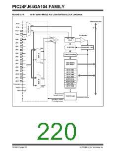
A block diagram of the A/D Converter is shown in
Figure 21-1.
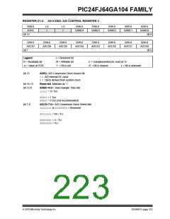
21.0 10-BIT HIGH-SPEED A/D
CONVERTER
To perform an A/D conversion:
Note:
This data sheet summarizes the features
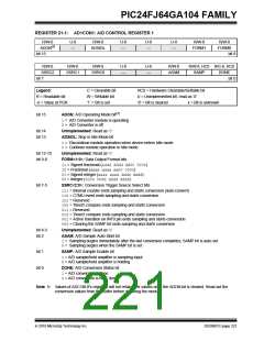
1. Configure the A/D module:
of this group of PIC24F devices. It is not
intended to be a comprehensive reference
source. For more information, refer to the
“PIC24F Family Reference Manual”,
Section 17. “10-Bit A/D Converter”
(DS39705).
a) Configure port pins as analog inputs and/or
select band gap reference inputs
(AD1PCFGL<15:0> and AD1PCFGH<1:0>).
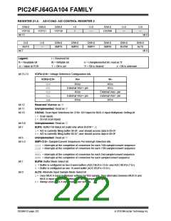
b) Select voltage reference source to match
expected range on analog inputs
(AD1CON2<15:13>).
The 10-bit A/D Converter has the following key
features:
c) Select the analog conversion clock to match
the desired data rate with the processor
clock (AD1CON3<7:0>).
• Successive Approximation (SAR) conversion
• Conversion speeds of up to 500 ksps
• 13 analog input pins
d) Select the appropriate sample/conversion
sequence
(AD1CON1<7:5>
and
AD1CON3<12:8>).
• External voltage reference input pins
• Internal band gap reference inputs
• Automatic Channel Scan mode
• Selectable conversion trigger source
• 16-word conversion result buffer
• Selectable Buffer Fill modes
e) Select how conversion results are
presented in the buffer (AD1CON1<9:8>).
f) Select interrupt rate (AD1CON2<5:2>).
g) Turn on A/D module (AD1CON1<15>).
2. Configure the A/D interrupt (if required):
a) Clear the AD1IF bit.
• Four result alignment options
b) Select A/D interrupt priority.
• Operation during CPU Sleep and Idle modes
On all PIC24FJ64GA104 family devices, the 10-bit A/D
Converter has 13 analog input pins, designated AN0
through AN12. In addition, there are two analog input
pins for external voltage reference connections (VREF+
and VREF-). These voltage reference inputs may be
shared with other analog input pins.
2010 Microchip Technology Inc.
DS39951C-page 219

 MICROCHIP [ MICROCHIP ]