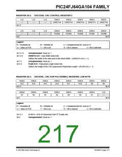
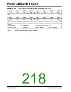
PIC24FJ64GA104 FAMILY
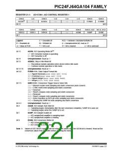
REGISTER 21-1: AD1CON1: A/D CONTROL REGISTER 1
R/W-0
ADON(1)
U-0
—
R/W-0
U-0
—
U-0
—
U-0
—
R/W-0
R/W-0
ADSIDL
FORM1
FORM0
bit 15
bit 8
R/W-0
R/W-0
R/W-0
U-0
—
U-0
—
R/W-0
ASAM
R/W-0, HCS R/C-0, HCS
SAMP DONE
bit 0
SSRC2
SSRC1
SSRC0
bit 7
Legend:
C = Clearable bit
W = Writable bit
‘1’ = Bit is set
HCS = Hardware Clearable/Settable bit
U = Unimplemented bit, read as ‘0’
R = Readable bit
-n = Value at POR
‘0’ = Bit is cleared
x = Bit is unknown
bit 15
ADON: A/D Operating Mode bit(1)
1= A/D Converter module is operating
0= A/D Converter is off
bit 14
bit 13
Unimplemented: Read as ‘0’
ADSIDL: Stop in Idle Mode bit
1= Discontinue module operation when device enters Idle mode
0= Continue module operation in Idle mode
bit 12-10
bit 9-8
Unimplemented: Read as ‘0’
FORM<1:0>: Data Output Format bits
11= Signed fractional (sddd dddd dd00 0000)
10= Fractional (dddd dddd dd00 0000)
01= Signed integer (ssss sssd dddd dddd)
00= Integer (0000 00dd dddd dddd)
bit 7-5
SSRC<2:0>: Conversion Trigger Source Select bits
111= Internal counter ends sampling and starts conversion (auto-convert)
110= CTMU event ends sampling and starts conversion
101= Reserved
100= Timer5 compare ends sampling and starts conversion
011= Reserved
010= Timer3 compare ends sampling and starts conversion
001= Active transition on INT0 pin ends sampling and starts conversion
000= Clearing the SAMP bit ends sampling and starts conversion
bit 4-3
bit 2
Unimplemented: Read as ‘0’
ASAM: A/D Sample Auto-Start bit
1= Sampling begins immediately after the last conversion completes; SAMP bit is auto-set
0= Sampling begins when the SAMP bit is set
bit 1
bit 0
SAMP: A/D Sample Enable bit
1= A/D sample/hold amplifier is sampling input
0= A/D sample/hold amplifier is holding
DONE: A/D Conversion Status bit
1= A/D conversion is done
0= A/D conversion is NOT done
Note 1: Values of ADC1BUFx registers will not retain their values once the ADON bit is cleared. Read out the
conversion values from the buffer before disabling the module.
2010 Microchip Technology Inc.
DS39951C-page 221

 MICROCHIP [ MICROCHIP ]