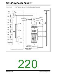
PIC24FJ64GA104 FAMILY
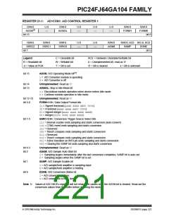
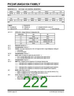
REGISTER 21-2: AD1CON2: A/D CONTROL REGISTER 2
R/W-0
R/W-0
R/W-0
r-0
r
U-0
—
R/W-0
U-0
—
U-0
—
VCFG2
VCFG1
VCFG0
CSCNA
bit 15
bit 8
R-0
U-0
—
R/W-0
SMPI3
R/W-0
SMPI2
R/W-0
SMPI1
R/W-0
SMPI0
R/W-0
BUFM
R/W-0
ALTS
BUFS
bit 7
bit 0
Legend:
r = Reserved bit
W = Writable bit
‘1’ = Bit is set
R = Readable bit
U = Unimplemented bit, read as ‘0’
‘0’ = Bit is cleared x = Bit is unknown
-n = Value at POR
bit 15-13
VCFG<2:0>: Voltage Reference Configuration bits
VCFG<2:0>
VR+
VR-
000
001
010
011
1xx
AVDD
External VREF+ pin
AVDD
AVSS
AVSS
External VREF- pin
External VREF- pin
AVSS
External VREF+ pin
AVDD
bit 12
bit 11
bit 10
Reserved: Maintain as ‘0’
Unimplemented: Read as ‘0’
CSCNA: Scan Input Selections for CH0+ S/H Input for MUX A Input Multiplexer Setting bit
1= Scan inputs
0= Do not scan inputs
bit 9-8
bit 7
Unimplemented: Read as ‘0’
BUFS: Buffer Fill Status bit (valid only when BUFM = 1)
1= A/D is currently filling buffer 08-0F; user should access data in 00-07
0= A/D is currently filling buffer 00-07; user should access data in 08-0F
bit 6
Unimplemented: Read as ‘0’
bit 5-2
SMPI<3:0>: Sample/Convert Sequences Per Interrupt Selection bits
1111 = Interrupts at the completion of conversion for each 16th sample/convert sequence
1110 = Interrupts at the completion of conversion for each 15th sample/convert sequence
.....
0001 = Interrupts at the completion of conversion for each 2nd sample/convert sequence
0000 = Interrupts at the completion of conversion for each sample/convert sequence
bit 1
bit 0
BUFM: Buffer Mode Select bit
1 = Buffer is configured as two 8-word buffers (ADC1BUFn<15:8> and ADC1BUFn<7:0>)
0 = Buffer is configured as one 16-word buffer (ADC1BUFn<15:0>)
ALTS: Alternate Input Sample Mode Select bit
1= Uses MUX A input multiplexer settings for first sample, then alternates between MUX B and
MUX A input multiplexer settings for all subsequent samples
0= Always uses MUX A input multiplexer settings
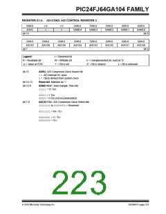
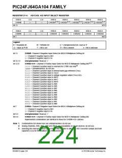
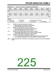
DS39951C-page 222
2010 Microchip Technology Inc.

 MICROCHIP [ MICROCHIP ]