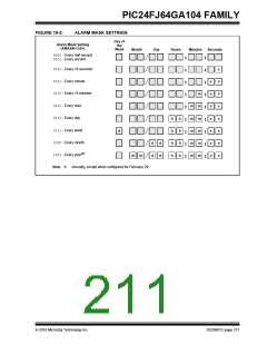
PIC24FJ64GA104 FAMILY
20.1.3
DATA SHIFT DIRECTION
20.2 Registers
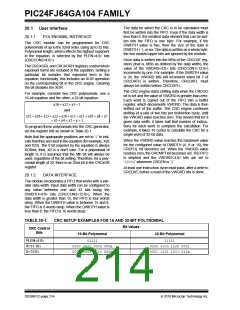
The LENDIAN bit (CRCCON1<3>) is used to control
the shift direction. By default, the CRC will shift data
through the engine, MSb first. Setting LENDIAN (= 1)
causes the CRC to shift data, LSb first. This setting
allows better integration with various communication
schemes and removes the overhead of reversing the
bit order in software. Note that this only changes the
direction of the data that is shifted into the engine. The
result of the CRC calculation will still be a normal CRC
result, not a reverse CRC result.
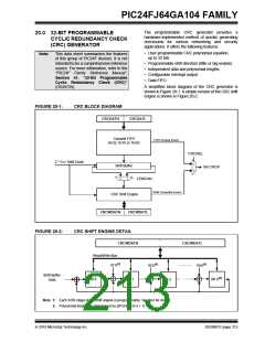
There are eight registers associated with the module:
• CRCCON1
• CRCCON2
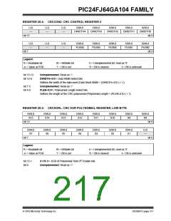
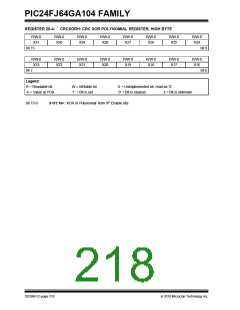
• CRCXORL
• CRCXORH
• CRCDATL
• CRCDATH
• CRCWDATL
• CRCWDATH
20.1.4
INTERRUPT OPERATION
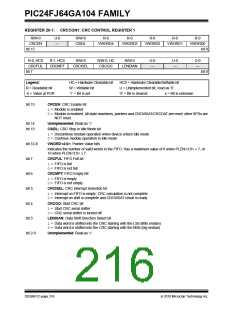
The
CRCCON1
and
CRCCON2
registers
The module generates an interrupt that is configurable
by the user for either of two conditions.
(Register 20-1 and Register 20-2) control the operation
of the module, and configure the various settings. The
CRCXOR registers (Register 20-3 and Register 20-4)
select the polynomial terms to be used in the CRC
equation. The CRCDAT and CRCWDAT registers are
each register pairs that serve as buffers for the
double-word, input data and CRC processed output,
respectively.
If CRCISEL is ‘0’, an interrupt is generated when the
VWORD<4:0> bits make a transition from a value of ‘1’
to ‘0’. If CRCISEL is ‘1’, an interrupt will be generated
after the CRC operation finishes and the module sets
the CRCGO bit to ‘0’. Manually setting CRCGO to ‘0’
will not generate an interrupt.
20.1.5
TYPICAL OPERATION
To use the module for a typical CRC calculation:
1. Set the CRCEN bit to enable the module.
2. Configure the module for the desired operation:
d) Program the desired polynomial using the
CRCXORL and CRCXORH registers, and
the PLEN<4:0> bits
e) Configure the data width and shift direction
using the DWIDTH and LENDIAN bits
f) Select the desired interrupt mode using the
CRCISEL bit
3. Preload the FIFO by writing to the CRCDATL
and CRCDATH registers until the CRCFUL bit is
set or no data is left
4. Clear old results by writing 00h to CRCWDATL
and CRCWDATH. CRCWDAT can also be left
unchanged to resume a previously halted
calculation.
5. Set the CRCGO bit to start calculation.
6. Write remaining data into the FIFO as space
becomes available.
7. When the calculation completes, CRCGO is
automatically cleared. An interrupt will be
generated if CRCISEL = 1.
8. Read CRCWDATL and CRCWDATH for the
result of the calculation.
2010 Microchip Technology Inc.
DS39951C-page 215

 MICROCHIP [ MICROCHIP ]