PIC24FJ64GA104 FAMILY
16.2 Setting Baud Rate When
Operating as a Bus Master
16.3 Slave Address Masking
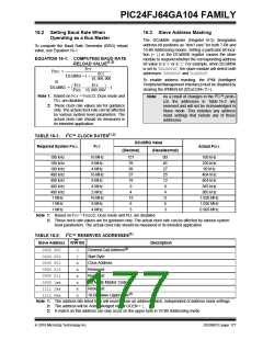
The I2CxMSK register (Register 16-3) designates
address bit positions as “don’t care” for both 7-Bit and
10-Bit Addressing modes. Setting a particular bit loca-
tion (= 1) in the I2CxMSK register causes the slave
module to respond whether the corresponding address
bit value is a ‘0’ or a ‘1’. For example, when I2CxMSK
is set to ‘00100000’, the slave module will detect both
addresses: ‘0000000’ and ‘0100000’.
To compute the Baud Rate Generator (BRG) reload
value, use Equation 16-1.
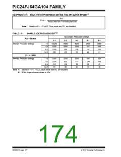
EQUATION 16-1: COMPUTING BAUD RATE
RELOAD VALUE(1,2)
FCY
FSCL = ---------------------------------------------------------------------
FCY
I2CxBRG + 1 + -----------------------------
10 000 000
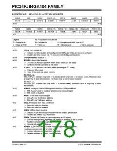
To enable address masking, the IPMI (Intelligent
Peripheral Management Interface) must be disabled by
clearing the IPMIEN bit (I2CxCON<11>).
or
FCY
FCY
I2CxBRG = ----------- – ----------------------------- – 1
FSCL 10 000 000
As a result of changes in the I2C™ proto-
col, the addresses in Table 16-2 are
reserved and will not be Acknowledged in
Slave mode. This includes any address
mask settings that include any of these
addresses.
Note 1: Based on FCY = FOSC/2, Doze mode and
PLL are disabled.
Note:
2: These clock rate values are for guidance
only. The actual clock rate can be affected
by various system level parameters. The
actual clock rate should be measured in
its intended application.
TABLE 16-1: I2C™ CLOCK RATES(1,2)
I2CxBRG Value
Required System FSCL
FCY
Actual FSCL
(Decimal)
(Hexadecimal)
9D
100 kHz
100 kHz
100 kHz
400 kHz
400 kHz
400 kHz
400 kHz
1 MHz
16 MHz
8 MHz
4 MHz
16 MHz
8 MHz
4 MHz
2 MHz
16 MHz
8 MHz
4 MHz
157
78
39
37
18
9
100 kHz
100 kHz
99 kHz
4E
27
25
12
9
404 kHz
404 kHz
385 kHz
385 kHz
1.026 MHz
1.026 MHz
0.909 MHz
4
4
13
6
D
1 MHz
6
1 MHz
3
3
Note 1: Based on FCY = FOSC/2, Doze mode and PLL are disabled.
2: These clock rate values are for guidance only. The actual clock rate can be affected by various system
level parameters. The actual clock rate should be measured in its intended application.
TABLE 16-2: I2C™ RESERVED ADDRESSES(1)
Slave Address R/W Bit
Description
0000 000
0000 000
0000 001
0000 010
0000 011
0000 1xx
1111 1xx
1111 0xx
0
1
x
x
x
x
x
x
General Call Address(2)
Start Byte
Cbus Address
Reserved
Reserved
HS Mode Master Code
Reserved
10-Bit Slave Upper Byte(3)
Note 1: The address bits listed here will never cause an address match, independent of address mask settings.
2: The address will be Acknowledged only if GCEN = 1.
3: A match on this address can only occur on the upper byte in 10-Bit Addressing mode.
2010 Microchip Technology Inc.
DS39951C-page 177

 MICROCHIP [ MICROCHIP ]