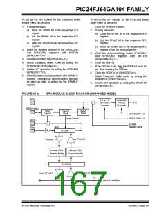
PIC24FJ64GA104 FAMILY
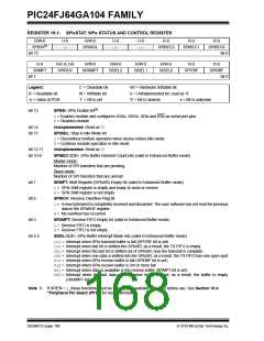
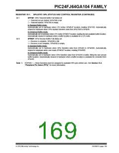
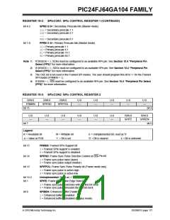
REGISTER 15-2: SPIXCON1: SPIx CONTROL REGISTER 1 (CONTINUED)
bit 4-2
SPRE<2:0>: Secondary Prescale bits (Master mode)
111= Secondary prescale 1:1
110= Secondary prescale 2:1
...
000= Secondary prescale 8:1
bit 1-0
PPRE<1:0>: Primary Prescale bits (Master mode)
11= Primary prescale 1:1
10= Primary prescale 4:1
01= Primary prescale 16:1
00= Primary prescale 64:1
Note 1: If DISSCK = 0, SCKx must be configured to an available RPn pin. See Section 10.4 “Peripheral Pin
Select (PPS)” for more information.
2: If DISSDO = 0, SDOx must be configured to an available RPn pin. See Section 10.4 “Peripheral Pin
Select (PPS)” for more information.
3: The CKE bit is not used in the Framed SPI modes. The user should program this bit to ‘0’ for the Framed
SPI modes (FRMEN = 1).
4: If SSEN = 1, SSx must be configured to an available RPn pin. See Section 10.4 “Peripheral Pin Select
(PPS)” for more information.
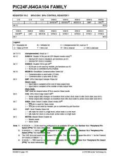
REGISTER 15-3: SPIxCON2: SPIx CONTROL REGISTER 2
R/W-0
R/W-0
R/W-0
U-0
—
U-0
—
U-0
—
U-0
—
U-0
—
FRMEN
SPIFSD
SPIFPOL
bit 15
bit 8
U-0
—
U-0
—
U-0
—
U-0
—
U-0
—
U-0
—
R/W-0
SPIFE
R/W-0
SPIBEN
bit 7
bit 0
Legend:
R = Readable bit
W = Writable bit
‘1’ = Bit is set
U = Unimplemented bit, read as ‘0’
‘0’ = Bit is cleared x = Bit is unknown
-n = Value at POR
bit 15
bit 14
bit 13
FRMEN: Framed SPIx Support bit
1= Framed SPIx support is enabled
0= Framed SPIx support is disabled
SPIFSD: Frame Sync Pulse Direction Control on SSx Pin bit
1= Frame sync pulse input (slave)
0= Frame sync pulse output (master)
SPIFPOL: Frame Sync Pulse Polarity bit (Frame mode only)
1= Frame sync pulse is active-high
0= Frame sync pulse is active-low
bit 12-2
bit 1
Unimplemented: Read as ‘0’
SPIFE: Frame Sync Pulse Edge Select bit
1= Frame sync pulse coincides with the first bit clock
0= Frame sync pulse precedes the first bit clock
bit 0
SPIBEN: Enhanced Buffer Enable bit
1= Enhanced buffer is enabled
0= Enhanced buffer is disabled (Legacy mode)
2010 Microchip Technology Inc.
DS39951C-page 171

 MICROCHIP [ MICROCHIP ]