PIC24FJ64GA104 FAMILY
10.4.6
PERIPHERAL PIN SELECT
REGISTERS
Note:
Input and output register values can only be
changed if IOLOCK (OSCCON<6>) = 0.
See Section 10.4.4.1 “Control Register
Lock” for a specific command sequence.
The PIC24FJ64GA104 family of devices implements a
total of 27 registers for remappable peripheral
configuration:
• Input Remappable Peripheral Registers (14)
• Output Remappable Peripheral Registers (13)
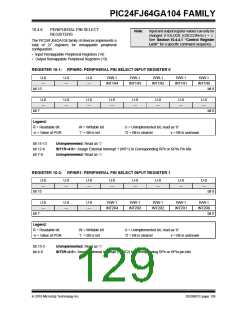
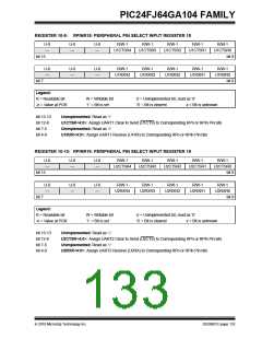
REGISTER 10-1: RPINR0: PERIPHERAL PIN SELECT INPUT REGISTER 0
U-0
—
U-0
—
U-0
—
R/W-1
R/W-1
R/W-1
R/W-1
R/W-1
INT1R4
INT1R3
INT1R2
INT1R1
INT1R0
bit 15
bit 8
U-0
—
U-0
—
U-0
—
U-0
—
U-0
—
U-0
—
U-0
—
U-0
—
bit 7
bit 0
Legend:
R = Readable bit
-n = Value at POR
W = Writable bit
‘1’ = Bit is set
U = Unimplemented bit, read as ‘0’
‘0’ = Bit is cleared x = Bit is unknown
bit 15-13
bit 12-8
bit 7-0
Unimplemented: Read as ‘0’
INT1R<4:0>: Assign External Interrupt 1 (INT1) to Corresponding RPn or RPIn Pin bits
Unimplemented: Read as ‘0’
REGISTER 10-2: RPINR1: PERIPHERAL PIN SELECT INPUT REGISTER 1
U-0
—
U-0
—
U-0
—
U-0
—
U-0
—
U-0
—
U-0
—
U-0
—
bit 15
bit 8
U-0
—
U-0
—
U-0
—
R/W-1
R/W-1
R/W-1
R/W-1
R/W-1
INT2R4
INT2R3
INT2R2
INT2R1
INT2R0
bit 7
bit 0
Legend:
R = Readable bit
-n = Value at POR
W = Writable bit
‘1’ = Bit is set
U = Unimplemented bit, read as ‘0’
‘0’ = Bit is cleared x = Bit is unknown
bit 15-5
bit 4-0
Unimplemented: Read as ‘0’
INT2R<4:0>: Assign External Interrupt 2 (INT2) to Corresponding RPn or RPIn pin bits
2010 Microchip Technology Inc.
DS39951C-page 129

 MICROCHIP [ MICROCHIP ]