PIC24FJ64GA104 FAMILY
9.2.4.3
Exiting Deep Sleep Mode
9.2.4.4
Deep Sleep Wake-up Time
Deep Sleep mode exits on any one of the following events:
Since wake-up from Deep Sleep results in a POR, the
wake-up time from Deep Sleep is the same as the
device POR time. Also, because the internal regulator
is turned off, the voltage on VCAP may drop depending
on how long the device is asleep. If VCAP has dropped
below 2V, then there will be additional wake-up time
while the regulator charges VCAP.
• POR event on VDD supply. If there is no DSBOR
circuit to re-arm the VDD supply POR circuit, the
external VDD supply must be lowered to the
natural arming voltage of the POR circuit.
• DSWDT time-out. When the DSWDT timer times
out, the device exits Deep Sleep.
Deep Sleep wake-up time is specified in Section 28.0
“Electrical Characteristics” as TDSWU. This specifi-
cation indicates the worst-case wake-up time, including
the full POR Reset time (including TPOR and TRST), as
well as the time to fully charge a 10 F capacitor on
VCAP which has discharged to 0V. Wake-up may be
significantly faster if VCAP has not discharged.
• RTCC alarm (if RTCEN = 1).
• Assertion (‘0’) of the MCLR pin.
• Assertion of the INT0 pin (if the interrupt was
enabled before Deep Sleep mode was entered).
The polarity configuration is used to determine the
assertion level (‘0’ or ‘1’) of the pin that will cause
an exit from Deep Sleep mode. Exiting from Deep
Sleep mode requires a change on the INT0 pin
while in Deep Sleep mode.
9.2.4.5
Saving Context Data with the
DSGPR0/DSGPR1 Registers
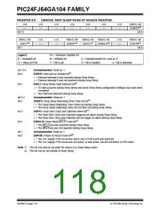
Note:
Any interrupt pending when entering Deep
Sleep mode is cleared.
As exiting Deep Sleep mode causes a POR, most
Special Function Registers reset to their default POR
values. In addition, because VDDCORE power is not
supplied in Deep Sleep mode, information in data RAM
may be lost when exiting this mode.
Exiting Deep Sleep mode generally does not retain the
state of the device and is equivalent to a Power-on
Reset (POR) of the device. Exceptions to this include
the RTCC (if present), which remains operational
through the wake-up, the DSGPRx registers and the
DSWDT bit.
Applications which require critical data to be saved
prior to Deep Sleep may use the Deep Sleep General
Purpose registers, DSGPR0 and DSGPR1, or data
EEPROM (if available). Unlike other SFRs, the con-
tents of these registers are preserved while the device
is in Deep Sleep mode. After exiting Deep Sleep,
software can restore the data by reading the registers
and clearing the RELEASE bit (DSCON<0>).
Wake-up events that occur from the time Deep Sleep
exits, until the time that the POR sequence completes,
are ignored, and are not captured in the DSWAKE
register.
The sequence for exiting Deep Sleep mode is:
1. After a wake-up event, the device exits Deep
Sleep and performs a POR. The DSEN bit is
cleared automatically. Code execution resumes
at the Reset vector.
9.2.4.6
I/O Pins During Deep Sleep
During Deep Sleep, the general purpose I/O pins retain
their previous states and the Secondary Oscillator
(SOSC) will remain running, if enabled. Pins that are
configured as inputs (TRIS bit is set) prior to entry into
Deep Sleep remain high-impedance during Deep
Sleep. Pins that are configured as outputs (TRIS bit is
clear) prior to entry into Deep Sleep remain as output
pins during Deep Sleep. While in this mode, they
continue to drive the output level determined by their
corresponding LAT bit at the time of entry into Deep
Sleep.
2. To determine if the device exited Deep Sleep,
read the Deep Sleep bit, DPSLP (RCON<10>).
This bit will be set if there was an exit from Deep
Sleep mode. If the bit is set, clear it.
3. Determine the wake-up source by reading the
DSWAKE register.
4. Determine if a DSBOR event occurred during
Deep Sleep mode by reading the DSBOR bit
(DSCON<1>).
5. If application context data has been saved, read
it back from the DSGPR0 and DSGPR1
registers.
6. Clear the RELEASE bit (DSCON<0>).
DS39951C-page 114
2010 Microchip Technology Inc.

 MICROCHIP [ MICROCHIP ]