PIC24FJ64GA104 FAMILY
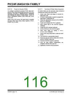
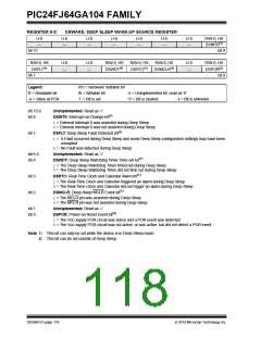
REGISTER 9-1:
R/W-0, HC
DSEN(1)
DSCON: DEEP SLEEP CONTROL REGISTER
U-0
—
U-0
—
U-0
—
U-0
—
U-0
—
U-0
—
U-0
—
bit 15
bit 8
U-0
—
U-0
—
U-0
—
U-0
—
U-0
—
U-0
—
R/W-0, HCS
R/C-0, HS
(1,2,3)
(1,2)
DSBOR
RELEASE
bit 7
bit 0
Legend:
R = Readable bit
-n = Value at POR
W = Writable bit
‘1’ = Bit is set
C = Clearable bit
‘0’ = Bit is cleared
U = Unimplemented, read as ‘0’
x = Bit is unknown
HC = Hardware Clearable bit HS = Hardware Settable bit HCS = Hardware Clearable/Settable bit
bit 15
DSEN: Deep Sleep Enable bit(1)
1= Device enters Deep Sleep when PWRSAV #0 is executed in the next instruction
0= Device enters normal Sleep when PWRSAV #0 is executed
bit 14-2
bit 1
Unimplemented: Read as ‘0’
DSBOR: Deep Sleep BOR Event Status bit(1,2,3)
1= The DSBOR was active and a BOR event was detected during Deep Sleep
0= The DSBOR was disabled or was active and did not detect a BOR event during Deep Sleep
bit 0
RELEASE: I/O Pin State Deep Sleep Release bit(1,2)
1= I/O pins and SOSC maintain their states following exit from Deep Sleep, regardless of their LAT
and TRIS configuration
0= I/O pins and SOSC are released from their Deep Sleep states. The pin state is controlled by the
LAT and TRIS configurations, and the SOSCEN bit.
Note 1: These bits are reset only in the case of a POR event outside of Deep Sleep mode.
2: Reset value is ‘0’ for initial power-on POR only and ‘1’ for Deep Sleep POR.
3: This is a status bit only; a DSBOR event will NOT cause a wake-up from Deep Sleep.
2010 Microchip Technology Inc.
DS39951C-page 117

 MICROCHIP [ MICROCHIP ]