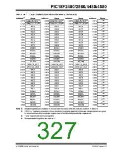
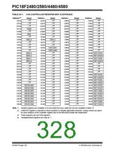
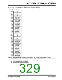
PIC18F2480/2580/4480/4580
24.3.4
LISTEN ONLY MODE
24.4 CAN Module Functional Modes
Listen Only mode provides
a
means for the
In addition to CAN modes of operation, the ECAN mod-
ule offers a total of 3 functional modes. Each of these
modes are identified as Mode 0, Mode 1 and Mode 2.
PIC18F2480/2580/4480/4580 devices to receive all
messages, including messages with errors. This mode
can be used for bus monitor applications or for
detecting the baud rate in ‘hot plugging’ situations. For
auto-baud detection, it is necessary that there are at
least two other nodes which are communicating with
each other. The baud rate can be detected empirically
by testing different values until valid messages are
received. The Listen Only mode is a silent mode,
meaning no messages will be transmitted while in this
state, including error flags or Acknowledge signals. The
filters and masks can be used to allow only particular
messages to be loaded into the receive registers or the
filter masks can be set to all zeros to allow a message
with any identifier to pass. The error counters are reset
and deactivated in this state. The Listen Only mode is
activated by setting the mode request bits in the
CANCON register.
24.4.1
MODE 0 – LEGACY MODE
Mode 0 is designed to be fully compatible with CAN
modules used in PIC18CXX8 and PIC18FXX8 devices.
This is the default mode of operation on all Reset con-
ditions. As a result, module code written for the
PIC18XX8 CAN module may be used on the ECAN
module without any code changes.
The following is the list of resources available in Mode 0:
• Three transmit buffers: TXB0, TXB1 and TXB2
• Two receive buffers: RXB0 and RXB1
• Two acceptance masks, one for each receive buf-
fer: RXM0, RXM1
• Six acceptance filters, 2 for RXB0 and 4 for RXB1:
RXF0, RXF1, RXF2, RXF3, RXF4, RXF5
24.3.5
LOOPBACK MODE
24.4.2
MODE 1 – ENHANCED LEGACY
MODE
This mode will allow internal transmission of messages
from the transmit buffers to the receive buffers without
actually transmitting messages on the CAN bus. This
mode can be used in system development and testing.
In this mode, the ACK bit is ignored and the device will
allow incoming messages from itself, just as if they
were coming from another node. The Loopback mode
is a silent mode, meaning no messages will be trans-
mitted while in this state, including error flags or
Acknowledge signals. The TXCAN pin will revert to port
I/O while the device is in this mode. The filters and
masks can be used to allow only particular messages
to be loaded into the receive registers. The masks can
be set to all zeros to provide a mode that accepts all
messages. The Loopback mode is activated by setting
the mode request bits in the CANCON register.
Mode 1 is similar to Mode 0, with the exception
that more resources are available in Mode 1. There are
16 acceptance filters and two acceptance mask regis-
ters. Acceptance Filter 15 can be used as either an
acceptance filter or an acceptance mask register. In
addition to three transmit and two receive buffers, there
are six more message buffers. One or more of these
additional buffers can be programmed as transmit or
receive buffers. These additional buffers can also be
programmed to automatically handle RTR messages.
Fourteen of sixteen acceptance filter registers can be
dynamically associated to any receive buffer and
acceptance mask register. One can use this capability
to associate more than one filter to any one buffer.
When a receive buffer is programmed to use standard
identifier messages, part of the full acceptance filter reg-
ister can be used as a data byte filter. The length of the
data byte filter is programmable from 0 to 18 bits. This
functionality simplifies implementation of high-level
protocols, such as the DeviceNet™ protocol.
24.3.6
ERROR RECOGNITION MODE
The module can be set to ignore all errors and receive
any message. In functional Mode 0, the Error Recogni-
tion mode is activated by setting the RXM<1:0> bits in
the RXBnCON registers to ‘11’. In this mode, the data
which is in the message assembly buffer until the error
time, is copied in the receive buffer and can be read via
the CPU interface.
The following is the list of resources available in Mode 1:
• Three transmit buffers: TXB0, TXB1 and TXB2
• Two receive buffers: RXB0 and RXB1
• Six buffers programmable as TX or RX: B0-B5
• Automatic RTR handling on B0-B5
• Sixteen dynamically assigned acceptance filters:
RXF0-RXF15
• Two dedicated acceptance mask registers;
RXF15 programmable as third mask:
RXM0-RXM1, RXF15
• Programmable data filter on standard identifier
messages: SDFLC
© 2009 Microchip Technology Inc.
DS39637D-page 331

 MICROCHIP [ MICROCHIP ]