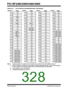
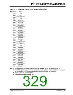
PIC18F2480/2580/4480/4580
Each receive buffer contains one Control register
(RXBnCON), four Identifier registers (RXBnSIDL,
RXBnSIDH, RXBnEIDL, RXBnEIDH), one Data Length
Count register (RXBnDLC) and eight Data Byte
registers (RXBnDm).
24.4.3
MODE 2 – ENHANCED FIFO MODE
In Mode 2, two or more receive buffers are used to form
the receive FIFO (first in, first out) buffer. There is no
one-to-one relationship between the receive buffer and
acceptance filter registers. Any filter that is enabled and
linked to any FIFO receive buffer can generate
acceptance and cause FIFO to be updated.
There is also a separate Message Assembly Buffer
(MAB) which acts as an additional receive buffer. MAB
is always committed to receiving the next message
from the bus and is not directly accessible to user firm-
ware. The MAB assembles all incoming messages one
by one. A message is transferred to appropriate
receive buffers only if the corresponding acceptance
filter criteria is met.
FIFO length is user-programmable, from 2-8 buffers
deep. FIFO length is determined by the very first pro-
grammable buffer that is configured as a transmit buf-
fer. For example, if Buffer 2 (B2) is programmed as a
transmit buffer, FIFO consists of RXB0, RXB1, B0 and
B1 – creating a FIFO length of 4. If all programmable
buffers are configured as receive buffers, FIFO will
have the maximum length of 8.
24.5.3
PROGRAMMABLE TRANSMIT/
RECEIVE BUFFERS
The following is the list of resources available in Mode 2:
The ECAN module implements six new buffers: B0-B5.
These buffers are individually programmable as either
transmit or receive buffers. These buffers are available
only in Mode 1 and 2. As with dedicated transmit and
receive buffers, each of these programmable buffers
occupies 14 bytes of SRAM and are mapped into SFR
memory map.
• Three transmit buffers: TXB0, TXB1 and TXB2
• Two receive buffers: RXB0 and RXB1
• Six buffers programmable as TX or RX; receive
buffers form FIFO: B0-B5
• Automatic RTR handling on B0-B5
• Sixteen acceptance filters: RXF0-RXF15
Each buffer contains one Control register (BnCON),
four Identifier registers (BnSIDL, BnSIDH, BnEIDL,
BnEIDH), one Data Length Count register (BnDLC)
and eight Data Byte registers (BnDm). Each of these
registers contains two sets of control bits. Depending
on whether the buffer is configured as transmit or
receive, one would use the corresponding control bit
set. By default, all buffers are configured as receive
buffers. Each buffer can be individually configured as a
transmit or receive buffer by setting the corresponding
TXENn bit in the BSEL0 register.
• Two dedicated acceptance mask registers;
RXF15 programmable as third mask:
RXM0-RXM1, RXF15
• Programmable data filter on standard identifier
messages: SDFLC, useful for DeviceNet protocol
24.5 CAN Message Buffers
24.5.1
DEDICATED TRANSMIT BUFFERS
The PIC18F2480/2580/4480/4580 devices implement
three dedicated transmit buffers – TXB0, TXB1 and
TXB2. Each of these buffers occupies 14 bytes of
SRAM and are mapped into the SFR memory map.
These are the only transmit buffers available in
Mode 0. Mode 1 and 2 may access these and other
additional buffers.
When configured as transmit buffers, user firmware
may access transmit buffers in any order similar to
accessing dedicated transmit buffers. In receive
configuration with Mode 1 enabled, user firmware may
also access receive buffers in any order required. But
in Mode 2, all receive buffers are combined to form a
single FIFO. Actual FIFO length is programmable by
user firmware. Access to FIFO must be done through
the FIFO Pointer bits (FP<4:0>) in the CANCON
register. It must be noted that there is no hardware
protection against out of order FIFO reads.
Each transmit buffer contains one Control register
(TXBnCON), four Identifier registers (TXBnSIDL,
TXBnSIDH, TXBnEIDL, TXBnEIDH), one Data Length
Count register (TXBnDLC) and eight Data Byte
registers (TXBnDm).
24.5.2
DEDICATED RECEIVE BUFFERS
The PIC18F2480/2580/4480/4580 devices implement
two dedicated receive buffers: RXB0 and RXB1. Each
of these buffers occupies 14 bytes of SRAM and are
mapped into SFR memory map. These are the only
receive buffers available in Mode 0. Mode 1 and 2 may
access these and other additional buffers.
DS39637D-page 332
© 2009 Microchip Technology Inc.

 MICROCHIP [ MICROCHIP ]