PIC18F2480/2580/4480/4580
The value in the ADRESH/ADRESL registers is not
2. Configure A/D interrupt (if desired):
• Clear ADIF bit
modified for a Power-on Reset. The ADRESH/ADRESL
registers will contain unknown data after a Power-on
Reset.
• Set ADIE bit
• Set GIE bit
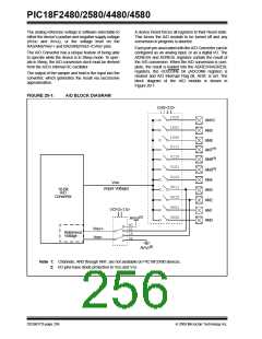
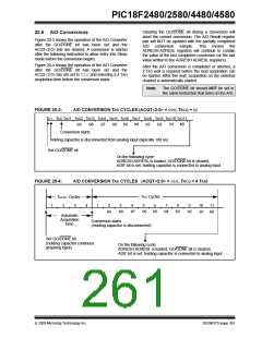
After the A/D module has been configured as desired,
the selected channel must be acquired before the con-
version is started. The analog input channels must
have their corresponding TRIS bits selected as an
input. To determine acquisition time, see Section 20.1
“A/D Acquisition Requirements”. After this acquisi-
tion time has elapsed, the A/D conversion can be
started. An acquisition time can be programmed to
occur between setting the GO/DONE bit and the actual
start of the conversion.
3. Wait the required acquisition time (if required).
4. Start conversion:
• Set GO/DONE bit (ADCON0 register)
5. Wait for A/D conversion to complete, by either:
• Polling for the GO/DONE bit to be cleared
OR
• Waiting for the A/D interrupt
6. Read A/D Result registers (ADRESH:ADRESL);
clear bit, ADIF, if required.
The following steps should be followed to perform an
A/D conversion:
7. For next conversion, go to step 1 or step 2, as
required. The A/D conversion time per bit is
defined as TAD. A minimum wait of 2 TAD is
required before next acquisition starts.
1. Configure the A/D module:
• Configure analog pins, voltage reference and
digital I/O (ADCON1)
• Select A/D input channel (ADCON0)
• Select A/D acquisition time (ADCON2)
• Select A/D conversion clock (ADCON2)
• Turn on A/D module (ADCON0)
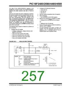
FIGURE 20-2:
ANALOG INPUT MODEL
VDD
Sampling
Switch
VT = 0.6V
ANx
SS
RIC ≤ 1k
RSS
Rs
CPIN
VAIN
ILEAKAGE
± 100 nA
CHOLD = 120 pF
VT = 0.6V
5 pF
VSS
Legend: CPIN
= Input Capacitance
= Threshold Voltage
6V
5V
VDD 4V
VT
ILEAKAGE = Leakage Current at the pin due to
various junctions
3V
RIC
= Interconnect Resistance
2V
SS
= Sampling Switch
CHOLD
RSS
= Sample/Hold Capacitance (from DAC)
= Sampling Switch Resistance
5
6
7
8 9 10 11
Sampling Switch (kΩ)
© 2009 Microchip Technology Inc.
DS39637D-page 257

 MICROCHIP [ MICROCHIP ]