PIC18F2480/2580/4480/4580
The module has five registers:
20.0 10-BIT ANALOG-TO-DIGITAL
• A/D Result High Register (ADRESH)
• A/D Result Low Register (ADRESL)
• A/D Control Register 0 (ADCON0)
• A/D Control Register 1 (ADCON1)
• A/D Control Register 2 (ADCON2)
CONVERTER (A/D) MODULE
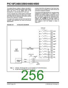
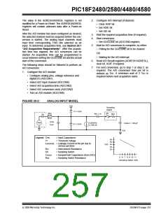
The Analog-to-Digital (A/D) Converter module has
8 inputs for the PIC18F2X80 devices and 11 for the
PIC18F4X80 devices. This module allows conversion
of an analog input signal to a corresponding 10-bit
digital number.
The ADCON0 register, shown in Register 20-1,
controls the operation of the A/D module. The
ADCON1 register, shown in Register 20-2, configures
the functions of the port pins. The ADCON2 register,
shown in Register 20-3, configures the A/D clock
source, programmed acquisition time and justification.
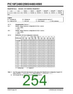
REGISTER 20-1: ADCON0: A/D CONTROL REGISTER 0
U-0
—
U-0
—
R/W-0
CHS3
R/W-0
CHS2
R/W-0
CHS1
R/W-0
CHS0
R/W-0
R/W-0
ADON
GO/DONE
bit 7
bit 0
Legend:
R = Readable bit
-n = Value at POR
W = Writable bit
‘1’ = Bit is set
U = Unimplemented bit, read as ‘0’
‘0’ = Bit is cleared x = Bit is unknown
bit 7-6
bit 5-2
Unimplemented: Read as ‘0’
CHS<3:0>: Analog Channel Select bits
0000= Channel 0 (AN0)
0001= Channel 1 (AN1)
0010= Channel 2 (AN2)
0011= Channel 3 (AN3)
0100= Channel 4 (AN4)
0101= Channel 5 (AN5)(1,2)
0110= Channel 6 (AN6)(1,2)
0111= Channel 7 (AN7)(1,2)
1000= Channel 8 (AN8)
1001= Channel 9 (AN9)
1010= Channel 10 (AN10)
1011= Unused
1100= Unused
1101= Unused
1110= Unused
1111= Unused
bit 1
bit 0
GO/DONE: A/D Conversion Status bit
When ADON = 1:
1= A/D conversion in progress
0= A/D Idle
ADON: A/D On bit
1= A/D Converter module is enabled
0= A/D Converter module is disabled
Note 1: These channels are not implemented on PIC18F2X80 devices.
2: Performing a conversion on unimplemented channels will return full-scale measurements.
© 2009 Microchip Technology Inc.
DS39637D-page 253

 MICROCHIP [ MICROCHIP ]