PIC18F2450/4450
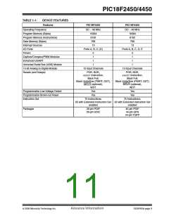
TABLE 1-2:
PIC18F2450 PINOUT I/O DESCRIPTIONS
Pin Number
Pin Buffer
Type Type
Pin Name
Description
PDIP,
QFN
SOIC
MCLR/Vpp/RE3
MCLR
1
Master Clear (input) or programming voltage (input).
Master Clear (Reset) input. This pin is an active-low
Reset to the device.
26
I
ST
ST
VPP
RE3
P
I
Programming voltage input.
Digital input.
OSC1/CLKI
OSC1
9
6
7
Oscillator crystal or external clock input.
I
I
Analog
Analog
Oscillator crystal input or external clock source input.
External clock source input. Always associated with pin
function OSC1. (See OSC2/CLKO pin.)
CLKI
OSC2/CLKO/RA6
OSC2
10
Oscillator crystal or clock output.
O
O
—
—
Oscillator crystal output. Connects to crystal or resonator
in Crystal Oscillator mode.
In select modes, OSC2 pin outputs CLKO which has
1/4 the frequency of OSC1 and denotes the instruction
cycle rate.
CLKO
RA6
I/O
TTL
General purpose I/O pin.
Legend: TTL = TTL compatible input
ST = Schmitt Trigger input with CMOS levels
= Output
CMOS = CMOS compatible input or output
I
= Input
O
P
= Power
DS39760A-page 12
Advance Information
© 2006 Microchip Technology Inc.

 MICROCHIP [ MICROCHIP ]