PIC18F2450/4450
1.2
Other Special Features
1.3
Details on Individual Family
Members
• Memory Endurance: The Enhanced Flash cells
for program memory are rated to last for many
thousands of erase/write cycles – up to 100,000.
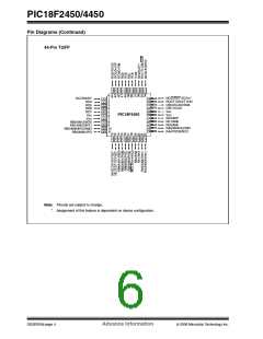
Devices in the PIC18F2450/4450 family are available
in 28-pin and 40/44-pin packages. Block diagrams for
the two groups are shown in Figure 1-1 and Figure 1-2.
• Self-Programmability: These devices can write
to their own program memory spaces under
internal software control. By using a bootloader
routine, located in the protected Boot Block at the
top of program memory, it becomes possible to
create an application that can update itself in the
field.
The devices are differentiated from each other in the
following two ways:
1. A/D channels (10 for 28-pin devices, 13 for
40/44-pin devices).
2. I/O ports (3 bidirectional ports and 1 input only
port on 28-pin devices, 5 bidirectional ports on
40/44-pin devices).
• Extended Instruction Set: The PIC18F2450/
4450 family introduces an optional extension to
the PIC18 instruction set, which adds 8 new
instructions and an Indexed
All other features for devices in this family are identical.
These are summarized in Table 1-1.
Literal Offset Addressing mode. This extension,
enabled as a device configuration option, has
been specifically designed to optimize re-entrant
application code originally developed in high-level
languages such as C.
The pinouts for all devices are listed in Table 1-2 and
Table 1-3.
Like all Microchip PIC18 devices, members of the
PIC18F2450/4450 family are available as both standard
and low-voltage devices. Standard devices with
Enhanced Flash memory, designated with an “F” in the
part number (such as PIC18F2450), accommodate an
operating VDD range of 4.2V to 5.5V. Low-voltage parts,
designated by “LF” (such as PIC18LF2450), function
over an extended VDD range of 2.0V to 5.5V.
• Enhanced Addressable USART: This serial
communication module is capable of standard
RS-232 operation and provides support for the LIN
bus protocol. Other enhancements include
Automatic Baud Rate Detection and a 16-bit Baud
Rate Generator for improved resolution.
• 10-Bit A/D Converter: This module incorporates
programmable acquisition time, allowing for a
channel to be selected and a conversion to be
initiated, without waiting for a sampling period and
thus, reducing code overhead.
• Dedicated ICD/ICSP Port: These devices
introduce the use of debugger and programming
pins that are not multiplexed with other micro-
controller features. Offered as an option in select
packages, this feature allows users to develop I/O
intensive applications while retaining the ability to
program and debug in the circuit.
DS39760A-page 8
Advance Information
© 2006 Microchip Technology Inc.

 MICROCHIP [ MICROCHIP ]