PIC18F2450/4450
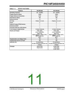
FIGURE 1-1:
PIC18F2450 (28-PIN) BLOCK DIAGRAM
Data Bus<8>
Table Pointer<21>
PORTA
RA0/AN0
RA1/AN1
Data Latch
8
8
inc/dec logic
21
RA2/AN2/VREF-
RA3/AN3/VREF+
RA4/T0CKI/RCV
RA5/AN4/HLVDIN
OSC2/CLKO/RA6
Data Memory
(2 Kbytes)
PCLATU PCLATH
Address Latch
20
PCU PCH PCL
Program Counter
12
Data Address<12>
31 Level Stack
STKPTR
4
BSR
12
FSR0
FSR1
FSR2
4
Address Latch
Access
Bank
Program Memory
(24/32 Kbytes)
12
Data Latch
PORTB
RB0/AN12/INT0
RB1/AN10/INT1
RB2/AN8/INT2/VMO
RB3/AN9/VPO
RB4/AN11/KBI0
RB5/KBI1/PGM
RB6/KBI2/PGC
RB7/KBI3/PGD
inc/dec
logic
8
Table Latch
Address
Decode
ROM Latch
IR
Instruction Bus <16>
8
Instruction
Decode &
Control
State Machine
Control Signals
PRODH PRODL
8 x 8 Multiply
PORTC
RC0/T1OSO/T1CKI
RC1/T1OSI/UOE
RC2/CCP1
RC4/D-/VM
RC5/D+/VP
3
8
OSC1(2)
OSC2(2)
T1OSI
Power-up
Timer
Internal
BITOP
8
W
Oscillator
Block
8
8
Oscillator
Start-up Timer
RC6/TX/CK
RC7/RX/DT
INTRC
Oscillator
8
8
Power-on
Reset
ALU<8>
8
Watchdog
Timer
T1OSO
Brown-out
Reset
MCLR(1)
VDD, VSS
Single-Supply
Programming
In-Circuit
Fail-Safe
Clock Monitor
Debugger
PORTE
Band Gap
Reference
USB Voltage
Regulator
VUSB
MCLR/VPP/RE3(1)
BOR
HLVD
ADC
10-bit
Timer0
Timer1
Timer2
EUSART
CCP1
USB
Note 1: RE3 is multiplexed with MCLR and is only available when the MCLR Resets are disabled.
2: OSC1/CLKI and OSC2/CLKO are only available in select oscillator modes and when these pins are not being used as digital I/O. Refer
to Section 2.0 “Oscillator Configurations” for additional information.
DS39760A-page 10
Advance Information
© 2006 Microchip Technology Inc.

 MICROCHIP [ MICROCHIP ]