PIC18CXX2
9.2.1
SWITCHING PRESCALER ASSIGNMENT
9.1
Timer0 Operation
The prescaler assignment is fully under software con-
trol, (i.e., it can be changed “on-the-fly” during program
execution).
Timer0 can operate as a timer or as a counter.
Timer mode is selected by clearing the T0CS bit. In
timer mode, the Timer0 module will increment every
instruction cycle (without prescaler). If the TMR0 regis-
ter is written, the increment is inhibited for the following
two instruction cycles. The user can work around this
by writing an adjusted value to the TMR0 register.
9.3
Timer0 Interrupt
The TMR0 interrupt is generated when the TMR0 reg-
ister overflows from FFh to 00h in 8-bit mode or FFFFh
to 0000h in 16-bit mode. This overflow sets the TMR0IF
bit. The interrupt can be masked by clearing the
TMR0IE bit. The TMR0IE bit must be cleared in soft-
ware by the Timer0 module interrupt service routine
before re-enabling this interrupt. The TMR0 interrupt
cannot awaken the processor from SLEEP, since the
timer is shut off during SLEEP.
Counter mode is selected by setting the T0CS bit. In
counter mode, Timer0 will increment either on every
rising or falling edge of pin RA4/T0CKI. The increment-
ing edge is determined by the Timer0 Source Edge
Select bit (T0SE). Clearing the T0SE bit selects the ris-
ing edge. Restrictions on the external clock input are
discussed below.
When an external clock input is used for Timer0, it must
meet certain requirements. The requirements ensure
the external clock can be synchronized with the internal
phase clock (TOSC). Also, there is a delay in the actual
incrementing of Timer0 after synchronization.
9.4
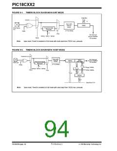
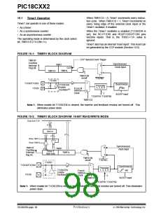
16-Bit Mode Timer Reads and Writes
TMR0H is not the high byte of the timer/counter in 16-
bit mode, but is actually a buffered version of the high
byte of Timer0 (refer to Figure 9-1). The high byte of
the Timer0 counter/timer is not directly readable nor
writable. TMR0H is updated with the contents of the
high byte of Timer0 during a read of TMR0L. This pro-
vides the ability to read all 16-bits of Timer0 without
having to verify that the read of the high and low byte
were valid due to a rollover between successive reads
of the high and low byte.
9.2
Prescaler
An 8-bit counter is available as a prescaler for the
Timer0 module. The prescaler is not readable or writ-
able.
The PSA and T0PS2:T0PS0 bits determine the pres-
caler assignment and prescale ratio.
A write to the high byte of Timer0 must also take place
through the TMR0H buffer register. Timer0 high byte is
updated with the contents of TMR0H when a write
occurs to TMR0L. This allows all 16 bits of Timer0 to
be updated at once.
Clearing bit PSA will assign the prescaler to the Timer0
module. When the prescaler is assigned to the Timer0
module, prescale values of 1:2, 1:4, ..., 1:256 are
selectable.
When assigned to the Timer0 module, all instructions
writing to the TMR0 register (e.g. CLRF TMR0,
MOVWF TMR0, BSF TMR0, x....etc.) will clear the
prescaler count.
Note: Writing to TMR0 when the prescaler is
assigned to Timer0 will clear the prescaler
count, but will not change the prescaler
assignment.
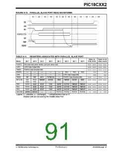
TABLE 9-1:
Name
REGISTERS ASSOCIATED WITH TIMER0
Value on Value on all
POR, BOR other resets
Bit 7
Timer0 Module’s Low Byte Register
TMR0H Timer0 Module’s High Byte Register
INTCON GIE/GIEH PEIE/GIEL TMR0IE INT0IE RBIE TMR0IF INT0IF RBIF
Bit 6
Bit 5
Bit 4
Bit 3
Bit 2
Bit 1
Bit 0
xxxx xxxx
0000 0000
0000 000x
1111 1111
--11 1111
uuuu uuuu
0000 0000
0000 000u
1111 1111
--11 1111
TMR0L
T0CON
TRISA
TMR0ON
—
T08BIT
—
T0CS
T0SE
PSA
T0PS2 T0PS1 T0PS0
PORTA Data Direction Register
Legend: x = unknown, u = unchanged, - = unimplemented locations read as '0'.
Shaded cells are not used by Timer0.
7/99 Microchip Technology Inc.
Preliminary
DS39026B-page 95

 MICROCHIP [ MICROCHIP ]