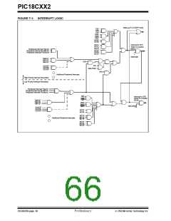
PIC18CXX2
7.0.2
PIR REGISTERS
7.0.3
PIE REGISTERS
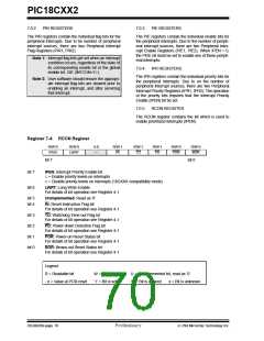
The PIR registers contain the individual flag bits for the
peripheral interrupts. Due to he number of peripheral
interrupt sources, there are two Peripheral Interrupt
Flag Registers (PIR1, PIR2).
The PIE registers contain the individual enable bits for
the peripheral interrupts. Due to the number of periph-
eral interrupt sources, there are two Peripheral Inter-
rupt Enable Registers (PIE1, PIE2). When IPEN = 0,
the PEIE bit must be set to enable any of these periph-
eral interrupts.
Note 1: Interrupt flag bits get set when an interrupt
condition occurs, regardless of the state of
its corresponding enable bit or the global
enable bit, GIE (INTCON<7>).
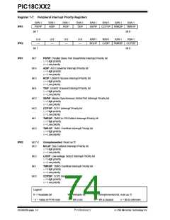
7.0.4
IPR REGISTERS
The IPR registers contain the individual priority bits for
the peripheral interrupts. Due to on the number of
peripheral interrupt sources, there are two Peripheral
Interrupt Priority Registers (IPR1, IPR2). The operation
of the priority bits requires that the Interrupt Priority
Enable (IPEN) bit be set.
Note 2: User software should ensure the appropri-
ate interrupt flag bits are cleared prior to
enabling an interrupt, and after servicing
that interrupt.
7.0.5
RCON REGISTER
The RCON register contains the bit which is used to
enable prioritized interrupts (IPEN).
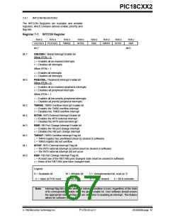
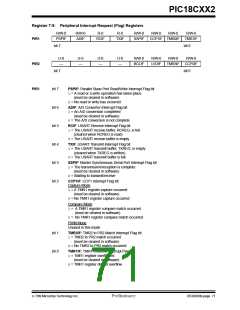
Register 7-4: RCON Register
R/W-0
IPEN
R/W-0
LWRT
U-0
R/W-1
R/W-1
R/W-1
R/W-0
R/W-0
—
RI
TO
PD
POR
BOR
bit 7
bit 0
bit 7
bit 6
IPEN: Interrupt Priority Enable bit
1= Enable priority levels on interrupts
0= Disable priority levels on interrupts (16CXXX compatibility mode)
LWRT: Long Write Enable
For details of bit operation see Register 4-1
bit 5
bit 4
Unimplemented: Read as ’0’
RI: Reset Instruction Flag bit
For details of bit operation see Register 4-1
bit 3
bit 2
bit 1
bit 0
TO: Watchdog Time-out Flag bit
For details of bit operation see Register 4-1
PD: Power-down Detection Flag bit
For details of bit operation see Register 4-1
POR: Power-on Reset Status bit
For details of bit operation see Register 4-1
BOR: Brown-out Reset Status bit
For details of bit operation see Register 4-1
Legend:
R = Readable bit
W = Writable bit
U = Unimplemented bit, read as ‘0’
’0’ = Bit is cleared x = Bit is unknown
- n = Value at POR reset
’1’ = Bit is set
DS39026B-page 70
Preliminary
7/99 Microchip Technology Inc.

 MICROCHIP [ MICROCHIP ]