PIC18CXX2
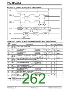
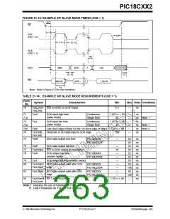
FIGURE 21-14: EXAMPLE SPI SLAVE MODE TIMING (CKE = 0)
SS
70
SCK
(CKP = 0)
83
71
72
78
79
79
SCK
(CKP = 1)
78
80
MSb
LSb
SDO
SDI
BIT6 - - - - - -1
77
75, 76
MSb IN
74
BIT6 - - - -1
LSb IN
73
Note: Refer to Figure 21-4 for load conditions.
TABLE 21-13: EXAMPLE SPI MODE REQUIREMENTS (SLAVE MODE TIMING (CKE = 0))
Parm.
Symbol
Characteristic
Min
Max Units Conditions
No.
70
TssL2scH, SS↓ to SCK↓ or SCK↑ input
TCY
—
ns
TssL2scL
71
TscH
TscL
SCK input high time
(slave mode)
Continuous
Single Byte
Continuous
Single Byte
1.25TCY + 30
—
—
—
—
—
ns
71A
72
40
1.25TCY + 30
40
ns Note 1
SCK input low time
(slave mode)
ns
72A
73
ns Note 1
ns
TdiV2scH, Setup time of SDI data input to SCK edge
TdiV2scL
100
73A
74
TB2B
Last clock edge of Byte1 to the 1st clock edge of Byte2 1.5TCY + 40
—
—
ns Note 2
ns
TscH2diL, Hold time of SDI data input to SCK edge
TscL2diL
100
75
TdoR
SDO data output rise time
PIC18CXXX
—
25
45
25
50
25
45
25
50
100
—
ns
ns
ns
ns
ns
ns
ns
ns
ns
ns
PIC18LCXXX
76
77
78
TdoF
SDO data output fall time
—
10
—
TssH2doZ SS↑ to SDO output hi-impedance
TscR
SCK output rise time
(master mode)
PIC18CXXX
PIC18LCXXX
79
80
TscF
SCK output fall time (master mode)
—
—
TscH2doV, SDO data output valid after SCK
TscL2doV edge
PIC18CXXX
PIC18LCXXX
83
TscH2ssH, SS ↑ after SCK edge
1.5TCY + 40
TscL2ssH
Note 1: Requires the use of Parameter # 73A.
2: Only if Parameter #s 71A and 72A are used.
DS39026B-page 262
Preliminary
7/99 Microchip Technology Inc.

 MICROCHIP [ MICROCHIP ]