PIC18CXX2
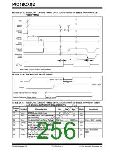
FIGURE 21-7: RESET, WATCHDOG TIMER, OSCILLATOR START-UP TIMER AND POWER-UP
TIMER TIMING
VDD
MCLR
30
Internal
POR
33
PWRT
Time-out
32
OSC
Time-out
Internal
Reset
Watchdog
Timer
Reset
31
34
34
I/O Pins
Note: Refer to Figure 21-4 for load conditions.
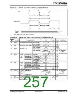
FIGURE 21-8: BROWN-OUT RESET TIMING
BVDD
VDD
35
VBGAP = 1.2V
VIRVST
Enable Internal Reference Voltage
Internal Reference Voltage stable
36
TABLE 21-7: RESET, WATCHDOG TIMER, OSCILLATOR START-UP TIMER, POWER-UP TIMER
AND BROWN-OUT RESET REQUIREMENTS
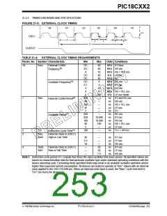
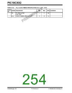
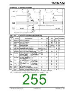
Param.
No.
Symbol
Characteristic
Min
Typ
Max
Units
Conditions
30
TmcL
MCLR Pulse Width (low)
2
—
—
µs
31
TWDT
Watchdog Timer Time-out Period
(No Prescaler)
7
18
33
ms
32
33
34
TOST
Oscillation Start-up Timer Period
1024TOSC
—
72
2
1024TOSC
132
—
ms
µs
TOSC = OSC1 period
TPWRT Power up Timer Period
28
—
TIOZ
I/O Hi-impedance from MCLR Low
—
or Watchdog Timer Reset
35
36
TBOR
TIVRST
Brown-out Reset Pulse Width
200
—
—
—
µs
µs
VDD ≤ BVDD (See
D005)
Time for Internal Reference
Voltage to become stable
20
50
DS39026B-page 256
Preliminary
7/99 Microchip Technology Inc.

 MICROCHIP [ MICROCHIP ]