PIC18CXX2
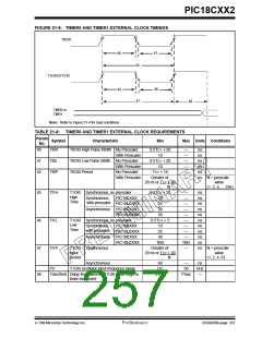
FIGURE 21-9: TIMER0 AND TIMER1 EXTERNAL CLOCK TIMINGS
T0CKI
41
40
42
T1OSO/T1CKI
46
45
47
48
TMR0 or
TMR1
Note: Refer to Figure 21-4 for load conditions.
TABLE 21-8: TIMER0 AND TIMER1 EXTERNAL CLOCK REQUIREMENTS
Param
Symbol
Characteristic
Min
Max Units Conditions
No.
40
Tt0H
T0CKI High Pulse Width No Prescaler
With Prescaler
0.5TCY + 20
10
—
—
—
—
—
—
ns
ns
ns
ns
ns
41
42
Tt0L
Tt0P
T0CKI Low Pulse Width No Prescaler
With Prescaler
0.5TCY + 20
10
T0CKI Period
No Prescaler
TCY + 10
With Prescaler
Greater of:
20 nS or TCY + 40
N
ns N = prescale
value
(1, 2, 4,..., 256)
45
46
Tt1H
Tt1L
T1CKI Synchronous, no prescaler
0.5TCY + 20
—
—
ns
ns
ns
ns
ns
ns
ns
ns
ns
ns
High
Time
Synchronous,
with prescaler
PIC18CXXX
10
PIC18LCXXX
25
—
Asynchronous PIC18CXXX
PIC18LCXXX
30
50
—
—
T1CKI Synchronous, no prescaler
0.5TCY + 5
10
—
Low
Time
Synchronous,
with prescaler
PIC18CXXX
—
PIC18LCXXX
25
—
Asynchronous PIC18CXXX
PIC18LCXXX
30
—
TBD
TBD
—
47
48
Tt1P
Ft1
T1CKI Synchronous
input
period
Greater of:
20 nS or TCY + 40
N
ns N = prescale
value
(1, 2, 4, 8)
Asynchronous
60
DC
—
50
ns
kHz
—
T1CKI oscillator input frequency range
Tcke2tmrI Delay from external T1CKI clock edge to
timer increment
2Tosc
7Tosc
7/99 Microchip Technology Inc.
Preliminary
DS39026B-page 257

 MICROCHIP [ MICROCHIP ]