PIC18CXX2
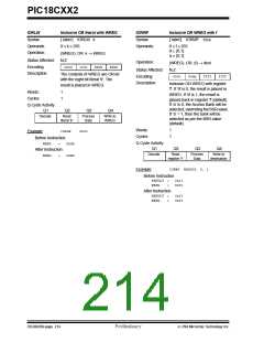
IORLW
IORWF
Inclusive OR literal with WREG
[ label ] IORLW k
0 ≤ k ≤ 255
Inclusive OR WREG with f
[ label ] IORWF f,d,a
0 ≤ f ≤ 255
Syntax:
Syntax:
Operands:
Operation:
Operands:
d
a
[0,1]
[0,1]
(WREG) .OR. k → WREG
Status Affected:
Encoding:
N,Z
Operation:
(WREG) .OR. (f) → dest
0000
1001
kkkk
kkkk
Status Affected:
Encoding:
N,Z
Description:
The contents of WREG are OR’ed
with the eight bit literal 'k'. The
result is placed in WREG.
0001
00da
ffff
ffff
Description:
Inclusive OR WREG with register
'f'. If 'd' is 0, the result is placed in
Words:
Cycles:
1
1
WREG. If 'd' is 1, the result is
placed back in register 'f' (default).
If ’a’ is 0, the Access Bank will be
selected, overriding the BSR value.
If ’a’ = 1, then the bank will be
selected as per the BSR value
(default).
Q Cycle Activity:
Q1
Q2
Q3
Q4
Decode
Read
literal ’k’
Process
Data
Write to
WREG
Words:
Cycles:
1
1
IORLW
0x9A
0x35
Example:
Before Instruction
Q Cycle Activity:
Q1
WREG
=
Q2
Q3
Q4
After Instruction
Decode
Read
register ’f’
Process
Data
Write to
destination
WREG
=
0xBF
IORWF RESULT, 0, 1
Example:
Before Instruction
RESULT
WREG
=
=
0x13
0x91
After Instruction
RESULT
WREG
=
=
0x13
0x93
DS39026B-page 214
Preliminary
7/99 Microchip Technology Inc.

 MICROCHIP [ MICROCHIP ]