PIC18CXX2
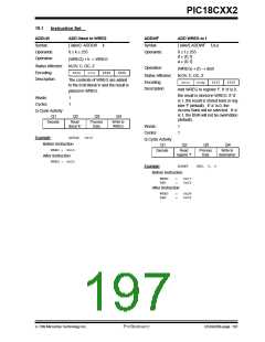
ADDWFC
ANDLW
ADD WREG and Carry bit to f
[ label ] ADDWFC f,d,a
0 ≤ f ≤ 255
AND literal with WREG
Syntax:
Syntax:
[ label ] ANDLW
0 ≤ k ≤ 255
k
Operands:
Operands:
Operation:
d
a
[0,1]
[0,1]
(WREG) .AND. k → WREG
Status Affected:
Encoding:
N,Z
Operation:
(WREG) + (f) + (C) → dest
0000
1011
kkkk
kkkk
Status Affected:
Encoding:
N,OV, C, DC, Z
Description:
The contents of WREG are AND’ed
with the 8-bit literal 'k'. The result is
placed in WREG.
0010
00da
ffff
ffff
Description:
Add WREG, the Carry Flag and data
memory location ’f’. If ’d’ is 0, the
Words:
Cycles:
1
1
result is placed in WREG. If ’d’ is 1,
the result is placed in data memory
location 'f'. If ’a’ is 0, the Access
Bank will be selected. If ’a’ is 1, the
BSR will not be overridden.
Q Cycle Activity:
Q1
Q2
Q3
Q4
Decode
Read literal
’k’
Process
Data
Write to
WREG
Words:
Cycles:
1
1
ANDLW
0x5F
Example:
Q Cycle Activity:
Q1
Before Instruction
Q2
Q3
Q4
WREG
=
0xA3
0x03
Decode
Read
register ’f’
Process
Data
Write to
destination
After Instruction
WREG
=
ADDWFC
REG, 0, 1
Example:
Before Instruction
Carry bit=
1
REG
=
=
0x02
WREG
0x4D
After Instruction
Carry bit=
0
REG
=
=
0x02
WREG
0x50
DS39026B-page 198
Preliminary
7/99 Microchip Technology Inc.

 MICROCHIP [ MICROCHIP ]