PIC18CXX2
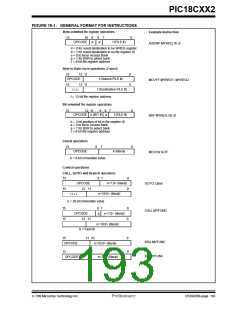
19.1
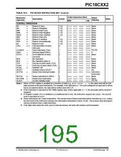
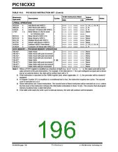
Instruction Set
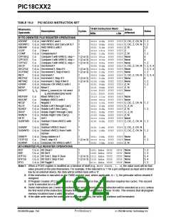
ADDLW
ADDWF
ADD literal to WREG
ADD WREG to f
Syntax:
[ label ] ADDLW
k
Syntax:
[ label ] ADDWF f,d,a
Operands:
Operation:
0 ≤ k ≤ 255
Operands:
0 ≤ f ≤ 255
d
a
[0,1]
[0,1]
(WREG) + k → WREG
Status Affected:
Encoding:
N,OV, C, DC, Z
Operation:
(WREG) + (f) → dest
0000
1111
kkkk
kkkk
Status Affected:
Encoding:
N,OV, C, DC, Z
Description:
The contents of WREG are added
to the 8-bit literal ’k’ and the result is
placed in WREG.
0010
01da
ffff
ffff
Description:
Add WREG to register ’f’. If ’d’ is 0,
the result is stored in WREG. If ’d’
is 1, the result is stored back in reg-
ister 'f' (default). If ’a’ is 0, the
Access Bank will be selected. If ’a’
is 1, the BSR will not be overridden
(default).
Words:
Cycles:
1
1
Q Cycle Activity:
Q1
Q2
Q3
Q4
Decode
Read
literal ’k’
Process
Data
Write to
WREG
Words:
Cycles:
1
1
ADDLW
0x15
Example:
Q Cycle Activity:
Q1
Before Instruction
Q2
Q3
Q4
WREG = 0x10
After Instruction
WREG = 0x25
Decode
Read
register ’f’
Process
Data
Write to
destination
ADDWF
REG, 0, 0
Example:
Before Instruction
WREG
REG
=
=
0x17
0xC2
After Instruction
WREG
REG
=
=
0xD9
0xC2
7/99 Microchip Technology Inc.
Preliminary
DS39026B-page 197

 MICROCHIP [ MICROCHIP ]