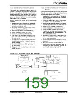
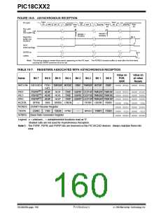
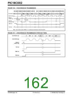
PIC18CXX2
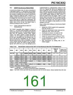
15.3.2 USART SYNCHRONOUS MASTER
RECEPTION
Steps to follow when setting up a Synchronous Master
Reception:
1. Initialize the SPBRG register for the appropriate
baud rate. (Section 15.1)
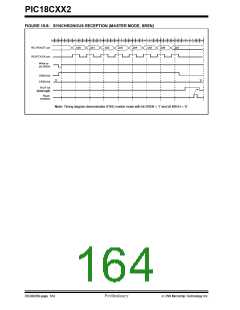
Once synchronous mode is selected, reception is
enabled by setting either enable bit SREN (RCSTA<5>)
or enable bit CREN (RCSTA<4>). Data is sampled on
the RC7/RX/DT pin on the falling edge of the clock. If
enable bit SREN is set, only a single word is received.
If enable bit CREN is set, the reception is continuous
until CREN is cleared. If both bits are set, then CREN
takes precedence.
2. Enable the synchronous master serial port by
setting bits SYNC, SPEN and CSRC.
3. Ensure bits CREN and SREN are clear.
4. If interrupts are desired, set enable bit RCIE.
5. If 9-bit reception is desired, set bit RX9.
6. If a single reception is required, set bit SREN.
For continuous reception, set bit CREN.
7. Interrupt flag bit RCIF will be set when reception
is complete and an interrupt will be generated if
the enable bit RCIE was set.
8. Read the RCSTA register to get the ninth bit (if
enabled) and determine if any error occurred
during reception.
9. Read the 8-bit received data by reading the
RCREG register.
10. If any error occurred, clear the error by clearing
bit CREN.
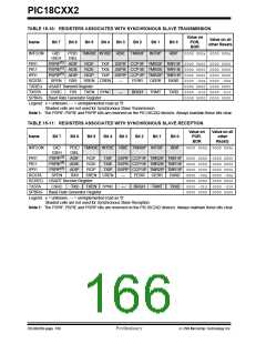
TABLE 15-9: REGISTERS ASSOCIATED WITH SYNCHRONOUS MASTER RECEPTION
Value on
POR,
BOR
Value on all
other
Resets
Name
Bit 7
Bit 6
Bit 5
Bit 4
Bit 3
Bit 2
Bit 1
Bit 0
INTCON
GIE/
GIEH
PEIE/ TMR0IE INT0IE RBIE TMR0IF INT0IF
GIEL
RBIF
0000 000x 0000 000u
PIR1
PSPIF(1) ADIF
PSPIE(1) ADIE
PSPIP(1) ADIP
RCIF
RCIE
RCIP
TXIF SSPIF CCP1IF TMR2IF TMR1IF 0000 0000 0000 0000
TXIE SSPIE CCP1IE TMR2IE TMR1IE 0000 0000 0000 0000
TXIP SSPIP CCP1IP TMR2IP TMR1IP 0000 0000 0000 0000
PIE1
IPR1
RCSTA
SPEN
RX9
SREN CREN
—
FERR
OERR
RX9D
0000 -00x 0000 -00x
0000 0000 0000 0000
0000 -010 0000 -010
0000 0000 0000 0000
RCREG USART Receive Register
TXSTA CSRC TX9 TXEN SYNC
SPBRG Baud Rate Generator Register
Legend: x = unknown, — = unimplemented read as '0'.
Shaded cells are not used for Synchronous Master Reception.
Note 1: The PSPIF, PSPIE and PSPIP bits are reserved on the PIC18C2X2 devices. Always maintain these bits clear.
—
BRGH
TRMT
TX9D
7/99 Microchip Technology Inc.
Preliminary
DS39026B-page 163

 MICROCHIP [ MICROCHIP ]