PIC18CXX2
enabled/disabled by setting/clearing enable bit TXIE
(PIE1<4>). Flag bit TXIF will be set, regardless of the
state of enable bit TXIE, and cannot be cleared in soft-
ware. It will reset only when new data is loaded into the
TXREG register. While flag bit TXIF indicates the status
of the TXREG register, another bit TRMT (TXSTA<1>)
shows the status of the TSR register. TRMT is a read
only bit, which is set when the TSR is empty. No inter-
rupt logic is tied to this bit, so the user has to poll this
bit in order to determine if the TSR register is empty.
The TSR is not mapped in data memory, so it is not
available to the user.
15.3
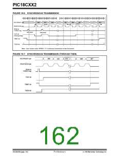
USART Synchronous Master Mode
In Synchronous Master mode, the data is transmitted in
a half-duplex manner, (i.e. transmission and reception
do not occur at the same time). When transmitting data,
the reception is inhibited and vice versa. Synchronous
mode is entered by setting bit SYNC (TXSTA<4>). In
addition, enable bit SPEN (RCSTA<7>) is set in order
to configure the RC6/TX/CK and RC7/RX/DT I/O pins
to CK (clock) and DT (data) lines respectively. The
Master mode indicates that the processor transmits the
master clock on the CK line. The Master mode is
entered by setting bit CSRC (TXSTA<7>).
Steps to follow when setting up a Synchronous Master
Transmission:
15.3.1 USART SYNCHRONOUS MASTER
TRANSMISSION
1. Initialize the SPBRG register for the appropriate
baud rate (Section 15.1).
The USART transmitter block diagram is shown in
Figure 15-1. The heart of the transmitter is the transmit
(serial) shift register (TSR). The shift register obtains its
data from the read/write transmit buffer register
TXREG. The TXREG register is loaded with data in
software. The TSR register is not loaded until the last
bit has been transmitted from the previous load. As
soon as the last bit is transmitted, the TSR is loaded
with new data from the TXREG (if available). Once the
TXREG register transfers the data to the TSR register
(occurs in one Tcycle), the TXREG is empty and inter-
rupt bit TXIF (PIR1<4>) is set. The interrupt can be
2. Enable the synchronous master serial port by
setting bits SYNC, SPEN, and CSRC.
3. If interrupts are desired, set enable bit TXIE.
4. If 9-bit transmission is desired, set bit TX9.
5. Enable the transmission by setting bit TXEN.
6. If 9-bit transmission is selected, the ninth bit
should be loaded in bit TX9D.
7. Start transmission by loading data to the
TXREG register.
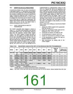
TABLE 15-8: REGISTERS ASSOCIATED WITH SYNCHRONOUS MASTER TRANSMISSION
Value on
Value on all
other Resets
Name
Bit 7
Bit 6
Bit 5
Bit 4
Bit 3
Bit 2
Bit 1
Bit 0
POR,
BOR
INTCON
GIE/
GIEH
PEIE/ TMR0IE INT0IE RBIE TMR0IF INT0IF
GIEL
RBIF
0000 000x
0000 000u
PIR1
PSPIF(1) ADIF
PSPIE(1) ADIE
PSPIP(1) ADIP
RCIF
RCIE
RCIP
TXIF SSPIF CCP1IF TMR2IF TMR1IF
TXIE SSPIE CCP1IE TMR2IE TMR1IE
TXIP SSPIP CCP1IP TMR2IP TMR1IP
0000 0000
0000 0000
0000 0000
0000 -00x
0000 0000
0000 -010
0000 0000
0000 0000
0000 0000
0000 0000
0000 -00x
0000 0000
0000 -010
0000 0000
PIE1
IPR1
RCSTA
SPEN
RX9
SREN CREN
—
FERR
OERR
RX9D
TXREG USART Transmit Register
TXSTA CSRC TX9 TXEN SYNC
SPBRG Baud Rate Generator Register
Legend: x = unknown, — = unimplemented, read as '0'.
Shaded cells are not used for Synchronous Master Transmission.
Note 1: The PSPIF, PSPIE and PSPIP bits are reserved on the PIC18C2X2 devices. Always maintain these bits clear.
—
BRGH
TRMT
TX9D
7/99 Microchip Technology Inc.
Preliminary
DS39026B-page 161

 MICROCHIP [ MICROCHIP ]