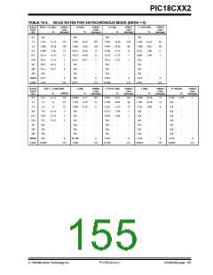
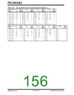
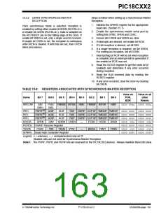
PIC18CXX2
15.2.2 USART ASYNCHRONOUS RECEIVER
15.2.3 SETTING UP 9-BIT MODE WITH ADDRESS
DETECT
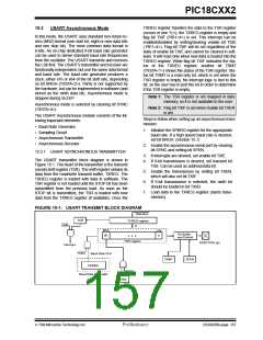
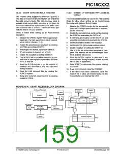
The receiver block diagram is shown in Figure 15-4.
The data is received on the RC7/RX/DT pin and drives
the data recovery block. The data recovery block is
actually a high speed shifter operating at x16 times the
baud rate, whereas the main receive serial shifter oper-
ates at the bit rate or at FOSC. This mode would typi-
cally be used in RS-232 systems.
This mode would typically be used in RS-485 systems.
Steps to follow when setting up an Asynchronous
Reception with Address Detect Enable:
1. Initialize the SPBRG register for the appropriate
baud rate. If a high speed baud rate is required,
set the BRGH bit.
Steps to follow when setting up an Asynchronous
Reception:
2. Enable the asynchronous serial port by clearing
the SYNC bit and setting the SPEN bit.
1. Initialize the SPBRG register for the appropriate
baud rate. If a high speed baud rate is desired,
set bit BRGH. (Section 15.1).
3. If interrupts are required, set the RCEN bit and
select the desired priority level with the RCIP bit.
4. Set the RX9 bit to enable 9-bit reception.
5. Set the ADDEN bit to enable address detect.
6. Enable reception by setting the CREN bit.
2. Enable the asynchronous serial port by clearing
bit SYNC and setting bit SPEN.
3. If interrupts are desired, set enable bit RCIE.
4. If 9-bit reception is desired, set bit RX9.
5. Enable the reception by setting bit CREN.
7. The RCIF bit will be set when reception is com-
plete. The interrupt will be acknowledged if the
RCIE and GIE bits are set.
6. Flag bit RCIF will be set when reception is com-
plete and an interrupt will be generated if enable
bit RCIE was set.
8. Read the RCSTA register to determine if any
error occurred during reception, as well as read
bit 9 of data (if applicable).
7. Read the RCSTA register to get the ninth bit (if
enabled) and determine if any error occurred
during reception.
9. Read RCREG to determine if the device is being
addressed.
10. If any error occurred, clear the CREN bit.
8. Read the 8-bit received data by reading the
RCREG register.
11. If the device has been addressed, clear the
ADDEN bit to allow all received data into the
receive buffer and interrupt the CPU.
9. If any error occurred, clear the error by clearing
enable bit CREN.
FIGURE 15-4: USART RECEIVE BLOCK DIAGRAM
x64 Baud Rate CLK
FERR
OERR
CREN
SPBRG
÷ 64
RSR Register
LSb
MSb
or
÷ 16
0
Baud Rate Generator
1
7
Stop (8)
Start
• • •
RC7/RX/DT
Pin Buffer
and Control
Data
Recovery
RX9
RX9D
SPEN
RCREG Register
FIFO
8
RCIF
RCIE
Interrupt
Data Bus
7/99 Microchip Technology Inc.
Preliminary
DS39026B-page 159

 MICROCHIP [ MICROCHIP ]