PIC18F6525/6621/8525/8621
7.5
Write Verify
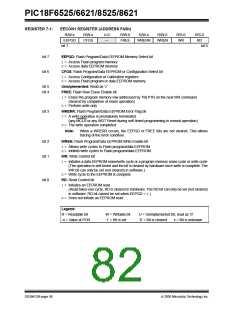
7.7
Operation During Code-Protect
Depending on the application, good programming
practice may dictate that the value written to the mem-
ory should be verified against the original value. This
should be used in applications where excessive writes
can stress bits near the specification limit.
Data EEPROM memory has its own code-protect
mechanism. External read and write operations are
disabled if either of these mechanisms are enabled.
Refer to Section 24.0 “Special Features of the
CPU”, for additional information.
7.6
Protection Against Spurious Write
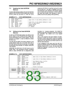
7.8
Using the Data EEPROM
There are conditions when the user may not want to
write to the data EEPROM memory. To protect against
spurious EEPROM writes, various mechanisms have
been built-in. On power-up, the WREN bit is cleared.
Also, the Power-up Timer (72 ms duration) prevents
EEPROM write.
The data EEPROM is a high endurance, byte
addressable array that has been optimized for the
storage of frequently changing information (e.g.,
program variables or other data that are updated
often). Frequently changing values will typically be
updated more often than specification D124. If this is
not the case, an array refresh must be performed. For
this reason, variables that change infrequently (such as
constants, IDs, calibration, etc.) should be stored in
Flash program memory.
The write initiate sequence and the WREN bit together
help prevent an accidental write during brown-out,
power glitch or software malfunction.
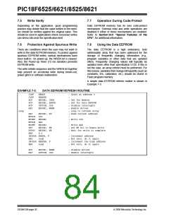
A simple data EEPROM refresh routine is shown in
Example 7-3.
EXAMPLE 7-3:
DATA EEPROM REFRESH ROUTINE
CLRF
CLRF
BCF
BCF
BCF
EEADR
EEADRH
EECON1, CFGS
EECON1, EEPGD
INTCON, GIE
EECON1, WREN
; Start at address 0
;
; Set for memory
; Set for Data EEPROM
; Disable interrupts
; Enable writes
; Loop to refresh array
; Read current address
;
; Write 55h
;
; Write AAh
; Set WR bit to begin write
; Wait for write to complete
BSF
Loop
BSF
EECON1, RD
55h
EECON2
AAh
EECON2
EECON1, WR
EECON1, WR
$-2
MOVLW
MOVWF
MOVLW
MOVWF
BSF
BTFSC
BRA
INCFSZ EEADR, F
; Increment address
BRA
Loop
; Not zero, do it again
; Increment the high address
; Not zero, do it again
INCFSZ EEADRH, F
BRA
Loop
BCF
BSF
EECON1, WREN
INTCON, GIE
; Disable writes
; Enable interrupts
DS39612B-page 82
2005 Microchip Technology Inc.

 MICROCHIP [ MICROCHIP ]