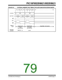
PIC18F6525/6621/8525/8621
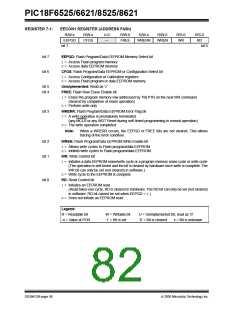
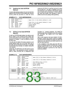
control bit (EECON1<6>) and then set the RD control
bit (EECON1<0>). The data is available for the very
next instruction cycle; therefore, the EEDATA register
7.3
Reading the Data EEPROM
Memory
To read a data memory location, the user must write the
address to the EEADRH:EEADR register pair, clear the
EEPGD control bit (EECON1<7>), clear the CFGS
can be read by the next instruction. EEDATA will hold
this value until another read operation or until it is
written to by the user (during a write operation).
EXAMPLE 7-1:
DATA EEPROM READ
MOVLW DATA_EE_ADDRH
;
MOVWF EEADRH
; Upper bits of Data Memory Address to read
MOVLW DATA_EE_ADDR
MOVWF EEADR
;
; Lower bits of Data Memory Address to read
; Point to DATA memory
; Access EEPROM
; EEPROM Read
; W = EEDATA
BCF
BCF
BSF
MOVF
EECON1, EEPGD
EECON1, CFGS
EECON1, RD
EEDATA, W
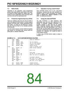
execution (i.e., runaway programs). The WREN bit
should be kept clear at all times except when updating
the EEPROM. The WREN bit is not cleared
by hardware.
7.4
Writing to the Data EEPROM
Memory
To write an EEPROM data location, the address must
first be written to the EEADRH:EEADR register pair
and the data written to the EEDATA register. Then the
sequence in Example 7-2 must be followed to initiate
the write cycle.
After a write sequence has been initiated, EECON1,
EEADRH, EEADR and EEDATA cannot be modified.
The WR bit will be inhibited from being set unless the
WREN bit is set. Both WR and WREN cannot be set
with the same instruction.
The write will not initiate if the above sequence is not
exactly followed (write 55h to EECON2, write AAh to
EECON2, then set WR bit) for each byte. It is strongly
recommended that interrupts be disabled during this
code segment.
At the completion of the write cycle, the WR bit is
cleared in hardware and the EEPROM Write Complete
Interrupt Flag bit (EEIF) is set. The user may either
enable this interrupt or poll this bit. EEIF must be
cleared by software.
Additionally, the WREN bit in EECON1 must be set to
enable writes. This mechanism prevents accidental
writes to data EEPROM due to unexpected code
EXAMPLE 7-2:
DATA EEPROM WRITE
MOVLW
DATA_EE_ADDRH
EEADRH
DATA_EE_ADDR
EEADR
DATA_EE_DATA
EEDATA
EECON1, EEPGD
EECON1, CFGS
EECON1, WREN
;
MOVWF
MOVLW
MOVWF
MOVLW
MOVWF
BCF
; Upper bits of Data Memory Address to write
;
; Lower bits of Data Memory Address to write
;
; Data Memory Value to write
; Point to DATA memory
; Access EEPROM
BCF
BSF
; Enable writes
BCF
INTCON, GIE
0x55
EECON2
0xAA
EECON2
; Disable Interrupts
;
; Write 55h
;
; Write AAh
; Set WR bit to begin write
; Enable Interrupts
MOVLW
MOVWF
MOVLW
MOVWF
BSF
Required
Sequence
EECON1, WR
INTCON, GIE
BSF
; User code execution
BCF
EECON1, WREN
; Disable writes on write complete (EEIF set)
2005 Microchip Technology Inc.
DS39612B-page 81

 MICROCHIP [ MICROCHIP ]