PIC17C4X
Applicable Devices 42 R42 42A 43 R43 44
Standard Operating Conditions (unless otherwise stated)
Operating temperature
-40˚C ≤ TA ≤ +85˚C for industrial and
0˚C ≤ TA ≤ +70˚C for commercial
Operating voltage VDD range as described in Section 17.1
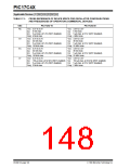
DC CHARACTERISTICS
Parameter
No.
Sym
Characteristic
Min
Typ†
Max Units
Conditions
Output Low Voltage
I/O ports (except RA2 and RA3)
with TTL buffer
D080
D081
VOL
–
–
–
–
0.1VDD
0.4
V
V
IOL = 4 mA
IOL = 6 mA, VDD = 4.5V
Note 6
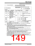
D082
D083
RA2 and RA3
OSC2/CLKOUT
–
–
–
–
3.0
0.4
V
V
IOL = 60.0 mA, VDD = 5.5V
IOL = 2 mA, VDD = 4.5V
(RC and EC osc modes)
Output High Voltage (Note 3)
D090
D091
VOH
I/O ports (except RA2 and RA3) 0.9VDD
–
–
–
–
V
V
IOH = -2 mA
IOH = -6.0 mA, VDD = 4.5V
Note 6
with TTL buffer
2.4
D092
D093
RA2 and RA3
–
–
–
12
–
V
V
Pulled-up to externally applied
voltage
IOH = -5 mA, VDD = 4.5V
OSC2/CLKOUT
2.4
(RC and EC osc modes)
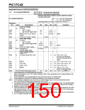
Capacitive Loading Specs on
Output Pins
D100
COSC2 OSC2 pin
–
–
25 ††
pF In EC or RC osc modes when
OSC2 pin is outputting
CLKOUT.
External clock is used to drive
OSC1.
D101
D102
CIO
All I/O pins and OSC2
(in RC mode)
System Interface Bus
(PORTC, PORTD and PORTE)
–
–
–
–
50 ††
pF
CAD
100 †† pF In Microprocessor or
Extended Microcontroller
mode
*
These parameters are characterized but not tested.
†
Data in “Typ” column is at 5V, 25°C unless otherwise stated. These parameters are for design guidance only
and are not tested.
‡
††
These parameters are for design guidance only and are not tested, nor characterized.
Design guidance to attain the AC timing specifications. These loads are not tested.
Note 1: In RC oscillator configuration, the OSC1 pin is a Schmitt Trigger input. It is not recommended that the
PIC17CXX devices be driven with external clock in RC mode.
2: The leakage current on the MCLR pin is strongly dependent on the applied voltage level. The specified levels
represent normal operating conditions. Higher leakage current may be measured at different input voltages.
3: Negative current is defined as coming out of the pin.
4: These specifications are for the programming of the on-chip program memory EPROM through the use of the
table write instructions. The complete programming specifications can be found in: PIC17CXX Programming
Specifications (Literature number DS30139).
5: The MCLR/Vpp pin may be kept in this range at times other than programming, but this is not recommended.
6: For TTL buffers, the better of the two specifications may be used.
1996 Microchip Technology Inc.
DS30412C-page 151

 MICROCHIP [ MICROCHIP ]