PIC17C4X
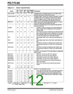
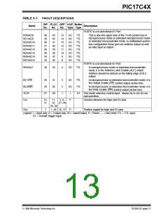
TABLE 3-1: PINOUT DESCRIPTIONS
DIP PLCC QFP I/O/P Buffer
Name
Description
No.
No.
No. Type Type
PORTD is a bi-directional I/O Port.
RD0/AD8
RD1/AD9
RD2/AD10
RD3/AD11
RD4/AD12
RD5/AD13
RD6/AD14
RD7/AD15
40
39
38
37
36
35
34
33
43
42
41
40
39
38
37
36
15
14
13
12
11
10
9
I/O
I/O
I/O
I/O
I/O
I/O
I/O
I/O
TTL
TTL
TTL
TTL
TTL
TTL
TTL
TTL
This is also the upper byte of the 16-bit system bus in
microprocessor mode or extended microprocessor mode
or extended microcontroller mode. In multiplexed system
bus configuration these pins are address output as well
as data input or output.
8
PORTE is a bi-directional I/O Port.
RE0/ALE
30
32
4
I/O
TTL
In microprocessor mode or extended microcontroller
mode, it is the Address Latch Enable (ALE) output.
Address should be latched on the falling edge of ALE
output.
RE1/OE
RE2/WR
TEST
29
28
27
31
30
29
11,
3
2
I/O
I/O
I
TTL
TTL
ST
In microprocessor or extended microcontroller mode, it is
the Output Enable (OE) control output (active low).
In microprocessor or extended microcontroller mode, it is
the Write Enable (WR) control output (active low).
1
Test mode selection control input. Always tie to VSS for nor-
mal operation.
VSS
10,
31
5, 6,
P
Ground reference for logic and I/O pins.
12, 27, 28
33, 34
VDD
1
1, 44 16, 17
P
Positive supply for logic and I/O pins.
Legend: I = Input only; O = Output only; I/O = Input/Output; P = Power; — = Not Used; TTL = TTL input;
ST = Schmitt Trigger input.
1996 Microchip Technology Inc.
DS30412C-page 13

 MICROCHIP [ MICROCHIP ]