PIC17C4X
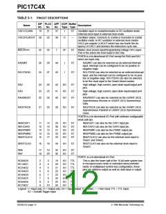
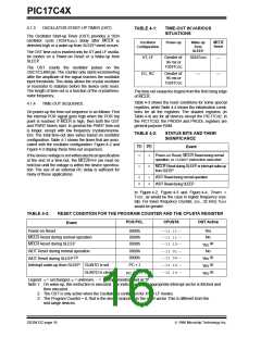
TABLE 3-1: PINOUT DESCRIPTIONS
DIP PLCC QFP I/O/P Buffer
Name
Description
No.
No.
No. Type Type
OSC1/CLKIN
19
21
37
38
I
ST
—
Oscillator input in crystal/resonator or RC oscillator mode.
External clock input in external clock mode.
OSC2/CLKOUT
20
32
22
35
O
Oscillator output. Connects to crystal or resonator in crystal
oscillator mode. In RC oscillator or external clock modes
OSC2 pin outputs CLKOUT which has one fourth the fre-
quency of OSC1 and denotes the instruction cycle rate.
MCLR/VPP
7
I/P
ST
Master clear (reset) input/Programming Voltage (VPP) input.
This is the active low reset input to the chip.
PORTA is a bi-directional I/O Port except for RA0 and RA1
which are input only.
RA0/INT
26
25
28
27
44
43
I
I
ST
ST
RA0/INT can also be selected as an external interrupt
input. Interrupt can be configured to be on positive or
negative edge.
RA1/T0CKI
RA1/T0CKI can also be selected as an external interrupt
input, and the interrupt can be configured to be on posi-
tive or negative edge. RA1/T0CKI can also be selected
to be the clock input to the Timer0 timer/counter.
RA2
24
23
22
26
25
24
42
41
40
I/O
I/O
I/O
ST
ST
ST
High voltage, high current, open drain input/output port
pins.
RA3
High voltage, high current, open drain input/output port
pins.
RA4/RX/DT
RA4/RX/DT can also be selected as the USART (SCI)
Asynchronous Receive or USART (SCI) Synchronous
Data.
RA5/TX/CK
21
23
39
I/O
ST
RA5/TX/CK can also be selected as the USART (SCI)
Asynchronous Transmit or USART (SCI) Synchronous
Clock.
PORTB is a bi-directional I/O Port with software configurable
weak pull-ups.
RB0/CAP1
RB1/CAP2
RB2/PWM1
RB3/PWM2
RB4/TCLK12
11
12
13
14
15
13
14
15
16
17
29
30
31
32
33
I/O
I/O
I/O
I/O
I/O
ST
ST
ST
ST
ST
RB0/CAP1 can also be the CAP1 input pin.
RB1/CAP2 can also be the CAP2 input pin.
RB2/PWM1 can also be the PWM1 output pin.
RB3/PWM2 can also be the PWM2 output pin.
RB4/TCLK12 can also be the external clock input to
Timer1 and Timer2.
RB5/TCLK3
16
18
34
I/O
ST
RB5/TCLK3 can also be the external clock input to
Timer3.
RB6
RB7
17
18
19
20
35
36
I/O
I/O
ST
ST
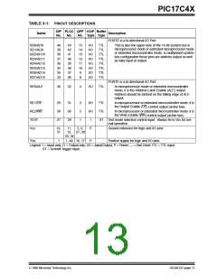
PORTC is a bi-directional I/O Port.
RC0/AD0
RC1/AD1
RC2/AD2
RC3/AD3
RC4/AD4
RC5/AD5
RC6/AD6
RC7/AD7
2
3
4
5
6
7
8
9
3
4
19
20
21
22
23
24
25
26
I/O
I/O
I/O
I/O
I/O
I/O
I/O
I/O
TTL
TTL
TTL
TTL
TTL
TTL
TTL
TTL
This is also the lower half of the 16-bit wide system bus
in microprocessor mode or extended microcontroller
mode. In multiplexed system bus configuration, these
pins are address output as well as data input or output.
5
6
7
8
9
10
Legend: I = Input only; O = Output only; I/O = Input/Output; P = Power; — = Not Used; TTL = TTL input;
ST = Schmitt Trigger input.
DS30412C-page 12
1996 Microchip Technology Inc.

 MICROCHIP [ MICROCHIP ]