PIC17C75X
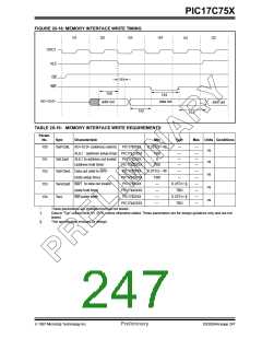
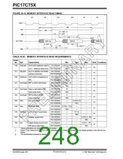
FIGURE 20-19: MEMORY INTERFACE READ TIMING
Q1
Q2
Q3
Q4
Q1
Q2
OSC1
166
ALE
OE
164
168
160
165
161
Data in
162
AD<15:0>
WR
Addr out
150
Addr out
151
163
167
'1'
'1'
TABLE 20-20: MEMORY INTERFACE READ REQUIREMENTS
Param.
No.
Sym
Characteristic
Min
Typ†
Max
Units Conditions
150
TadV2alL AD15:AD0 (address) valid to
PIC17CXXX 0.25Tcy - 10
—
—
ns
ALE↓ (address setup time) PIC17LCXXX
TBD
5*
—
—
—
—
—
—
151
160
TalL2adI
ALE↓ to address out invalid
PIC17CXXX
ns
ns
ns
ns
(address hold time)
PIC17LCXXX
TBD
TadZ2oeL AD15:AD0 hi-impedance to
OE↓
PIC17CXXX
0*
—
—
—
—
—
—
—
—
—
—
—
—
—
—
—
PIC17LCXXX
TBD
161
162
ToeH2adD OE↑ to AD15:AD0 driven
PIC17CXXX 0.25Tcy - 15
PIC17LCXXX
PIC17CXXX
PIC17LCXXX
PIC17CXXX
TBD
35
TadV2oeH Data in valid before OE↑
(data setup time)
TBD
0
163
164
165
ToeH2adI OE↑to data in invalid
(data hold time)
ns
ns
PIC17LCXXX
PIC17CXXX
PIC17LCXXX
TBD
—
—
—
—
TalH
ALE pulse width
0.25TCY §
TBD
—
ToeL
OE pulse width
PIC17CXXX 0.5Tcy - 35 §
—
—
ns
ns
ns
PIC17LCXXX
PIC17CXXX
PIC17LCXXX
PIC17CXXX
PIC17LCXXX
TBD
—
—
TCY §
TBD
—
—
166
167
TalH2alH ALE↑ to ALE↑(cycle time)
—
—
—
Tacc
Toe
Address access time
—
0.75TCY - 30
TBD
—
—
168
Output enable access time
(OE low to Data Valid)
PIC17CXXX
—
—
—
—
0.5TCY - 45
TBD
ns
PIC17LCXXX
*
These parameters are characterized but not tested.
†
Data in “Typ” column is at 5V, 25°C unless otherwise stated. These parameters are for design guidance only and are not
tested.
§
This specification ensured by design.
DS30264A-page 248
Preliminary
1997 Microchip Technology Inc.

 MICROCHIP [ MICROCHIP ]