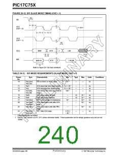
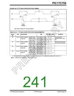
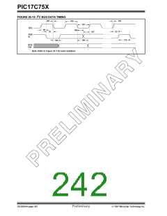
PIC17C75X
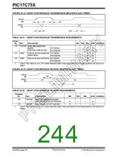
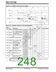
FIGURE 20-15: USART SYNCHRONOUS TRANSMISSION (MASTER/SLAVE) TIMING
TX/CK
pin
121
121
RX/DT
pin
122
120
TABLE 20-15: USART SYNCHRONOUS TRANSMISSION REQUIREMENTS
Param.
No.
Sym
Characteristic
Min Typ† Max Units Conditions
120
TckH2dtV SYNC XMIT (MASTER &
SLAVE)
PIC17CXXX
—
—
—
—
—
—
—
—
—
—
—
—
50
75 *
25
ns
ns
ns
ns
ns
ns
Clock high to data out valid
PIC17LCXXX
121
122
†
TckRF
TdtRF
Clock out rise time and fall time PIC17CXXX
(Master Mode)
PIC17LCXXX
40 *
25
Data out rise time and fall time PIC17CXXX
PIC17LCXXX
40 *
Data in “Typ” column is at 5V, 25°C unless otherwise stated. These parameters are for design guidance only and are not
tested.
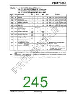
FIGURE 20-16: USART SYNCHRONOUS RECEIVE (MASTER/SLAVE) TIMING
TX/CK
125
pin
RX/DT
pin
126
TABLE 20-16: USART SYNCHRONOUS RECEIVE REQUIREMENTS
Parameter
No.
Sym
Characteristic
Min
Typ†
Max
Units Conditions
125
TdtV2ckL
SYNC RCV (MASTER & SLAVE)
Data hold before CK↓ (DT hold time)
15
15
—
—
—
—
ns
ns
126
TckL2dtl
Data hold after CK↓ (DT hold time)
†
Data in “Typ” column is at 5V, 25°C unless otherwise stated. These parameters are for design guidance only and are not
tested.
DS30264A-page 244
Preliminary
1997 Microchip Technology Inc.

 MICROCHIP [ MICROCHIP ]